
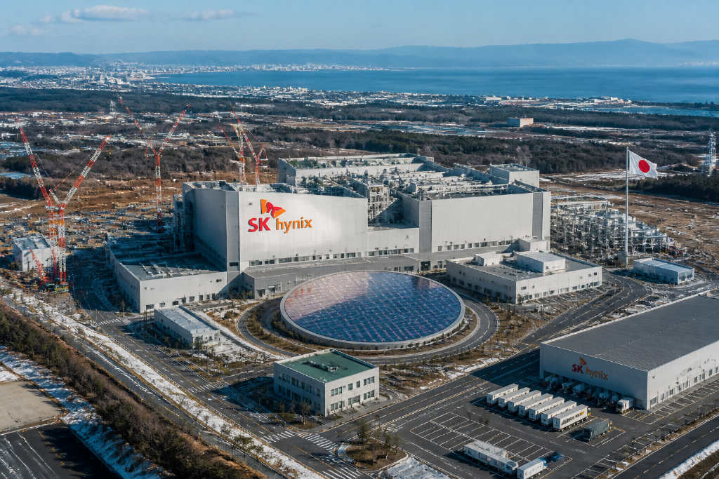
SK Hynix is reportedly pushing forward with a plan to invest several trillion won in a memory chip wafer plant in Miyagi Prefecture in northeastern Japan, according to a post on X by Citrini analyst jukan, who cited people familiar with the matter.
If the project goes ahead, it would become the first large-scale investment by a South Korean semiconductor company to establish a local manufacturing base in Japan. As the Japan investment plan advances, the report said the United States is also expected to increase pressure on South Korean companies to expand memory chip capacity in the U.S., adding complexity to future investment allocation decisions.
The Hankyoreh reported Aug. 20 that SK Hynix is seeking a site in Miyagi
The Hankyoreh reported on Aug. 20 that SK Hynix is seeking to build a memory chip wafer plant in Miyagi, located in the Tohoku region of Japan’s main island of Honshu.
One business source said, 「As I understand it, SK Group Chairman Chey Tae-won personally visited the area recently.」
Miyagi is one of three regions, together with Kyushu and Hokkaido, that the Japanese government plans to foster as major semiconductor industry centers. The report said the project’s investment size is expected to reach several trillion won.
Plant in Japan would be smaller than domestic cluster projects
Compared with the hundreds of trillions of won tied to domestic semiconductor cluster investments in Yongin and Honam, the Japan plant would be a relatively smaller production base.
The Miyagi wafer plant would serve as an additional overseas manufacturing base, while SK Hynix would continue with its existing plans to invest in the Yongin and Honam semiconductor clusters. The plan appears aimed at expanding production capacity as the global shortage of memory chips continues.
Could become the third foreign chipmaker operating manufacturing facilities in Japan
If the plan materializes, SK Hynix would become the third foreign semiconductor company to operate manufacturing facilities in Japan, after U.S.-based Micron and Taiwan’s TSMC.
Samsung Electronics currently operates only an advanced semiconductor packaging research center in Yokohama.
Plan carries pressure from Washington and sensitivity at home
The investment also comes with risks. The United States has been pressuring the South Korean government and South Korean companies to invest in memory chip wafer plants on U.S. soil. If SK Hynix proceeds with the Japan investment, Washington may press it to expand local production capacity in the United States as well.
SK Hynix must also contend with political uncertainty in South Korea, along with social sensitivity surrounding investment in Japan in strategic industries such as semiconductors.