
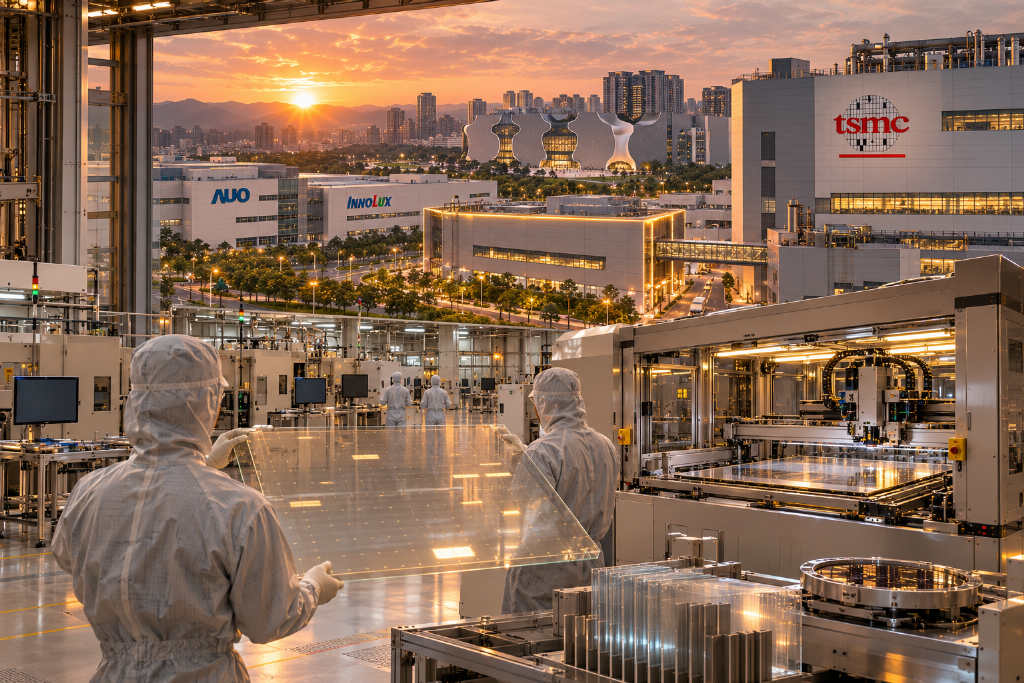
Taiwan Semiconductor Manufacturing Co. is pushing ahead with CoPoS panel-level packaging while continuing to buy panel-maker facilities, putting display manufacturers in the spotlight as potential suppliers for advanced packaging. Last week, TSMC said it would acquire AUO’s plant and related facilities in the Central Taiwan Science Park for NT$38.8 billion. At the same time, AUO is reportedly planning a glass-substrate pilot line to enter the CoPoS advanced-packaging supply chain, and Innolux is said to be moving in the same direction.
TSMC buys a second panel plant within two years
According to a report by Commercial Times, the AUO facility acquired by TSMC has about 166,000 ping of floor area, or roughly 548,800 square meters. AUO estimates it will book about NT$18.5 billion in disposal gains from the sale.
Including TSMC’s 2024 purchase of an Innolux plant in Tainan for NT$17.14 billion, the chipmaker’s total spending across the two panel-factory transactions has reached NT$55.94 billion. Supply-chain sources cited in the report said TSMC had previously sent staff several times to assess AUO’s L7A and L5C plants and had referred to the renovation experience from the Innolux facility. Engineering contractors estimated construction could begin as early as the second quarter of next year, though process configuration and mass-production timing have not been disclosed.
Taking over existing facilities is seen as a practical way to shorten the lead time needed before a new plant can be brought into operation.
CoPoS is aimed at larger AI chip packages
As demand for AI GPUs and high-performance computing keeps pushing package sizes higher, existing advanced-packaging technologies are nearing their limits. CoPoS is TSMC’s next-generation panel-level packaging technology. Instead of packaging diced chips on round wafers, the process packages them on square panels.
The report says square panels generate little corner waste. On the same area basis, they can produce five to six times as many chips as mainstream 300 mm round wafers, giving them a clear capacity advantage for AI chips.
TSMC chairman C.C. Wei previously said on an earnings call that competition in next-generation advanced packaging is gradually shifting from CoWoS to CoPoS. He said the company has already mass-produced packaging at 5x reticle size and is continuing toward 9x and 14x. He also said customers still prefer CoWoS for now and that TSMC will continue to provide sufficient capacity.
Glass core substrates represent a related but separate technology path. The report says their advantages include high flatness, dimensional stability and lower signal loss, which can help address warpage and transmission issues.
AUO and Innolux are both reported to be building out glass-substrate capabilities
Among panel makers, AUO is seen as one of the companies best positioned to benefit. The report says AUO is planning pilot lines for TGV, RDL and glass core substrates, using Corning glass and supporting a 510×515 mm substrate format. At this year’s SEMICON Taiwan, AUO and Corning jointly displayed a glass core substrate in that size.
On capital spending, AUO’s board recently approved an additional NT$5.728 billion for production-line optimization and new technology deployment at its innovation research institute. Still, AUO chairman Paul Peng said in July that glass core technology would need another two to three years before reaching a more mature stage and would be unlikely to contribute revenue in the short term.
At the same time, the report cited supply-chain sources saying Nvidia is testing glass core substrates and plans to have Innolux handle the front-end TGV process. Innolux’s 620×670 mm panel format was described as the largest in the industry and capable of supporting panel-level packaging with multilayer RDL as well as advanced packaging applications similar to CoPoS-L.
Global suppliers are evaluating the technology, but yield and qualification remain key hurdles
Interest in glass substrates is also building outside Taiwan. The report says Broadcom has partnered with TOPPAN to develop glass core substrates for its next-generation Tomahawk switch chip, using a 510×510 mm specification. South Korean media also reported that Nvidia has asked substrate makers in South Korea, Japan and Taiwan to complete development within two years, targeting adoption before 2028.
Industry participants cited in the report said process yield and customer qualification are the biggest challenges for moving glass substrates into large-scale commercialization. Another variable is asset disposal. AUO’s plan to sell its Huaya plant to Quanta for NT$19.7 billion was terminated after the two sides failed to reach agreement on usage specifications and delivery timing, showing that asset sales can still face uncertainty.
Whether AUO can use asset activation, pilot lines or technology partnerships to capture demand tied to TSMC’s CoWoS and CoPoS plans, and whether AUO and Innolux can secure customer qualification, remains to be seen.