
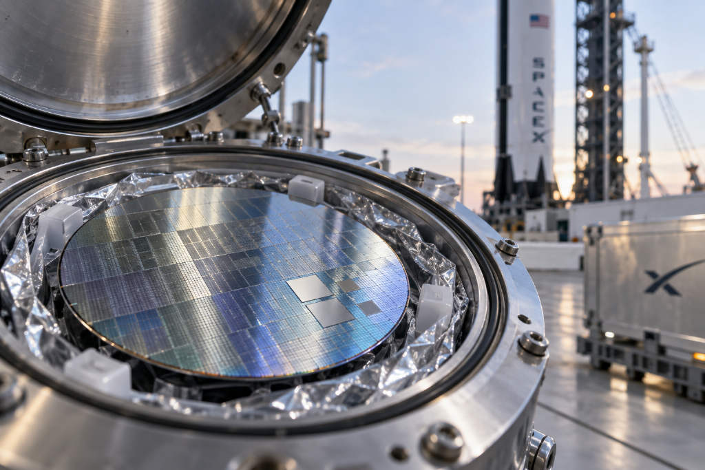
Besxar, a startup founded by former OpenAI employee Ashley Pilipiszyn, has begun testing a prototype for semiconductor manufacturing in space, using SpaceX Falcon 9 missions to validate the concept.
The company’s core argument is that semiconductor production should be moved to an environment where the relevant physical conditions already exist, rather than recreated on Earth through extremely expensive infrastructure.
Using space instead of rebuilding vacuum conditions on Earth
Pilipiszyn, Besxar’s founder and CEO, previously worked at OpenAI. She said terrestrial fabs become enormous and highly complex infrastructure projects because they require positive-pressure cleanrooms designed to block even tiny particles and contaminants. A single dust particle landing on a wafer can ruin the chip.
“We’re in an era where going to a place where the laws of physics are already working in our favor is actually more cost-effective than trying to fight physics here on Earth,” Pilipiszyn said. “Don’t fight physics on Earth.”
In Besxar’s view, the vacuum of space provides a level of purity that ground-based cleanrooms struggle to match, which is essential for protecting sensitive materials from contamination. Instead of spending billions of dollars to recreate a near-vacuum environment on Earth, the company wants to use space itself as the cleanroom.
The deeper attraction of manufacturing in space, according to the report, is microgravity. In terrestrial melting processes, thermal convection can disturb atomic arrangement like a mixer, creating crystal defects. In microgravity, atoms can arrange themselves more quietly, and the resulting compound semiconductor crystals may be more ordered. The report says electrical efficiency could be 10x to 100x higher than for Earth-made products.
Space Forge has made a similar case
Another startup targeting space-based semiconductor production, Space Forge, has expressed a similar view. Josh Western, the company’s founder and CEO, previously said vacuum and microgravity in space can support more effective development of entirely new semiconductor materials.
“Compound semiconductor growth is a very intensive and slow process, and they’re effectively grown from the atomic level,” Western said. “Gravity has a profound effect on them and fundamentally changes the bonds between those atoms. In space, you can overcome that barrier, because there’s almost no gravity.”
Western added that space offers a better manufacturing foundation for almost any material. By combining microgravity with high-purity vacuum without the need for multistage pumps, he said, access to space could enable roughly a billion new alloy combinations, along with extreme temperatures ranging from -260°C to 260°C, allowing researchers to make semiconductors “10 to 100 times more efficient than semiconductors on Earth.”
First flight returned wafer samples intact
In October 2025, Besxar reached an agreement with SpaceX to validate its orbital semiconductor manufacturing prototype over about 12 Falcon 9 flights. The goal is to test whether the natural vacuum of space can stand in for costly cleanroom infrastructure on Earth.
On July 5, 2026, Besxar’s first mission, Mission Asimov, launched aboard a SpaceX Falcon 9 booster. Two V1 Fabship manufacturing pods flew suborbitally and carried compound semiconductor wafer samples including GaAs and AlInAsSb from the University of Texas at Austin and the University of Virginia.
The two “Clipper-class” containers, described as microwave-sized modules, were designed as modular manufacturing units that use attributes of space such as vacuum, microgravity, and thermal conditions as process inputs. They were mounted to the Falcon 9 booster rather than placed into orbit, and returned to Earth with the booster after several minutes of suborbital flight.
The test objectives were to verify that the containers could survive launch loads, protect wafer samples from contamination, and expose the samples to the vacuum of space. According to Compound Semiconductor, post-flight inspection showed the structures remained intact and the wafers had no cracks, no warping, and no visible damage.
Pilipiszyn said the flown samples were the cleanest and had the lowest particulate counts compared with wafers that had not gone to space. “That’s very ideal for us as we think about scaling,” she said. Independent material-level analysis of the compound semiconductor wafer samples is still underway.
A staged roadmap from heating to deposition
Besxar’s roadmap is incremental. Over the next two years, the company plans to increase the complexity of its experiments in three stages.
- Stage one: heat wafers and verify in-space thermal management.
- Stage two: deposit one material and demonstrate basic thin-film growth.
- Stage three: expand to two or more materials and move closer to actual semiconductor manufacturing processes.
Its long-term objective is to place larger manufacturing modules on Starship, the launch system still under development at SpaceX. Pilipiszyn said that when she first approached SpaceX three years ago, the original discussions centered on launching with Starship, but Besxar ultimately chose to start with Falcon 9 booster rides to reduce technical risk at a more controllable cost.
Once it can produce qualified samples, Besxar plans to supply wafers to major chipmakers for advanced chips used in data centers, robotics, and electric vehicles, specifically in power regulation applications. The report says this positioning avoids direct competition with TSMC and Samsung in logic process technology and instead focuses on power semiconductors, where material purity is especially important.
Still, the gap between an engineering demonstration and commercial manufacturing remains large. A Falcon 9 booster’s suborbital profile provides only a few minutes of vacuum exposure, while real semiconductor thin-film deposition may require hours or longer in a controlled environment. It is also still unclear when Starship will be able to operate routinely at low cost.
Funding, contracts, and a growing field
Besxar has raised nearly $14 million to date, including a $9 million seed round co-led by Dauntless Ventures and Overture VC, with participation from Keymaker VC, 645 Ventures, and others. The company has also received early support from NVIDIA Inception and has begun work under a U.S. Department of Defense contract focused on defense-grade materials and radiation-hardened components.
Besxar is not alone in the field. United Semiconductors and Space Forge are also exploring how space conditions might be used to make higher-quality semiconductors.
All of them face the same bottleneck: getting enough product back to Earth. Pilipiszyn expects output per factory to grow from hundreds of wafers to thousands over time, but that path depends heavily on the availability of low-cost rockets, whether from SpaceX’s Starship or new vehicles under development by Rocket Lab, Stoke Space, and others.
A separate research effort funded by the U.S. CHIPS Act and NASA’s In Space Production Applications program is also studying semiconductor manufacturing in space. Its principal investigator is Curtis Hill, a senior materials engineer at NASA, whose team has used microgravity to simplify etching steps in semiconductor production.
The report also notes that the president of Japanese foundry Rapidus recently said in a speech in the United States that the company plans to build a semiconductor factory on the lunar surface around 2040.
From making wafers in space to deploying compute in space
If companies like Besxar are focused on making wafers in space, the Terafab plan announced by Elon Musk in March 2026 points in a different direction: deploying computing capacity in space.
According to the report, Terafab is a joint project involving Tesla, SpaceX, and xAI. Tesla described it as “the largest chip manufacturing factory in history,” with a target of producing 1 terawatt of AI compute chips per year, equivalent to 50 times current annual global AI compute output. The project is meant to collapse the conventional division of chipmaking by concentrating mask production, fabrication, packaging, and testing in a single site and creating a rapid iteration loop of mask creation, fabrication, testing, mask optimization, and remanufacturing.
The report says Musk explicitly placed Terafab’s strategic focus in space, citing natural limits on energy and compute on Earth. The high-power custom chips produced for the project would be tailored for extreme space environments and deployed in SpaceX’s orbital AI data center network.
Four practical obstacles highlighted in the report
An editor’s note in the original article argued that the logic behind making chips in space is sound, but several major questions remain unresolved.
1. Equipment suited for space does not yet exist at scale
There is still no established equipment stack designed specifically for semiconductor production in space. Sending existing semiconductor tools into orbit would be expensive and may not meet actual mission requirements. Installation would also be difficult. Lithography systems, for example, are physically massive and can weigh tens of tons, and even on Earth they can take months to install and calibrate. Unless equipment makers such as ASML build specialized space-compatible versions, the cost barrier remains high.
That said, some teams are already testing compact hardware. Nitride Global, working with United Semiconductors and Axiom Space, was selected for NASA’s SBIR program to develop a physical vapor deposition reactor for growing aluminum nitride, or AlN, crystals in microgravity. Its proof-of-concept reactor reportedly consumes 250 to 400 watts, weighs less than 700 grams, can operate at 2800°C to 3200°C, and fits the integration limits of an International Space Station middeck locker.
The report notes that the compound semiconductor growth Besxar is pursuing is inherently easier to miniaturize than lithography-heavy logic chip production. Even so, if the goal is a complete “space wafer fab,” deposition, etching, metrology, and other tool chains would still require major engineering adaptation.
2. Material supply and return logistics are unresolved
Even if a space-based semiconductor production line becomes technically ready, it would still need a stable supply of raw materials. If those materials must be launched continuously from Earth, cost and transit time become structural problems, especially for fabs that normally run 24/7.
After production, finished goods must also secure return capacity. The article says a Dragon cargo spacecraft can bring back only about 3,000 kilograms of downmass per mission, and scheduling is tied to International Space Station rotation cycles rather than a manufacturer’s own production cadence. Industry analysis cited in the report says return logistics have already “reshaped the economics of the entire emerging industry.” The market for return services is estimated at $1.5 billion to $1.8 billion in 2026 and could grow to $3.5 billion by 2030.
3. Radiation is a concern, but perhaps not the defining one
High-energy particles in space can alter crystal lattice structures in chips, leaving vacancy defects or interstitial defects that degrade performance or cause failure.
Still, the report cites research suggesting that for a 200 mm wafer, effective radiation damage under no electric field is below 10 rad and can be repaired through a simple annealing process. It also points to Google’s Project Suncatcher, where a Trillium AI chip survived testing equivalent to the radiation dose from a five-year low Earth orbit mission. That would imply radiation may pose a smaller threat to wafers during manufacturing than to finished chips operating in space over long periods. In the report’s framing, heat management and logistics remain more central obstacles.
4. The endgame may be local use in space, not return to Earth
The article also raises a broader possibility: the final form of space semiconductor manufacturing may not be shipping wafers back to Earth at all, but using them where they are made. In that model, a space factory would directly supply space infrastructure and form a closed loop that depends less on terrestrial logistics.
Although Musk’s Terafab project is described as being built mainly on Earth, its product positioning is explicitly tied to SpaceX’s orbital AI data center network. If orbital data centers, satellite constellations, and space manufacturing platforms scale up, then chips, boards, and thermal systems made in orbit could potentially be assembled and deployed there as well, bypassing the downmass bottleneck. The report notes that this would require chipmaking, board manufacturing, and packaging and testing capacity to move into space too, which is no smaller a challenge than chip fabrication itself.
For now, Besxar’s stated position is still to supply wafers to terrestrial chipmakers, which keeps it on a “made in space, used on Earth” track. A true closed loop would require much more of the supply chain to move off-planet.
Near-term focus remains on high-value, small-volume materials
The article concludes that the industrial logic of space semiconductor manufacturing is real, but the bottleneck is not whether chips can be made there. The bigger issues are whether suitable space manufacturing equipment can be built, whether raw materials can be supplied reliably, and whether the economics can become competitive. In the near term, the more practical path is likely high-value, small-volume growth of compound semiconductor materials rather than full-scale logic chip production.
The original article was sourced from the WeChat account Xinzhixun, edited by Xinzhixun-Langkejian and written by Xinzhixun-Langkejian, under the title: “Making Semiconductors in Space: This Company Has Already Started Testing.”