
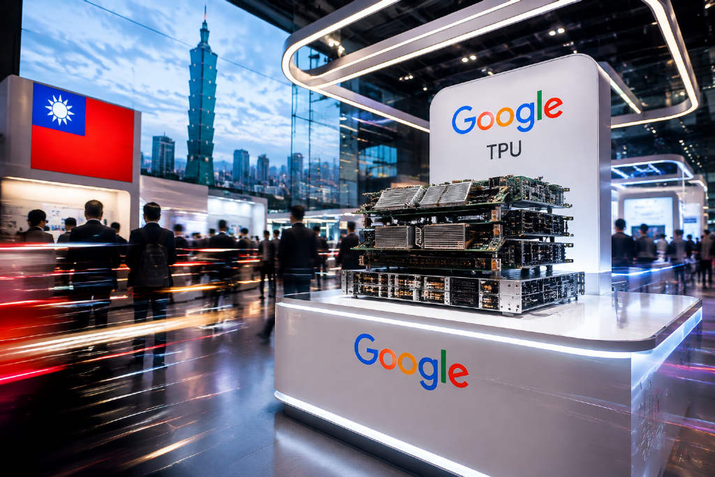
Morgan Stanley estimates that Google’s TPU business could generate $108 billion in annual revenue by 2028, based on deployment pricing, backlog and shipment volume. At that size, the unit would be large enough to rank among the world’s biggest semiconductor companies.

Omer Cheema, a semiconductor industry veteran who previously worked at Samsung, Advanced Micro Devices and Renesas Electronics, wrote that Google TPU is no longer just a tool for speeding up internal AI workloads. In his view, it is becoming a chip business that can stand on its own.
Google used SEMICON Taiwan to outline a faster TPU roadmap
On Sept. 2, Amin Vahdat, senior vice president and chief technology officer for Google AI infrastructure, took the stage at the opening keynote of SEMICON Taiwan. In what the article described as his first public speech in Asia, he said Google has compressed its TPU release cadence from one generation every two years to one generation every year, and is actively pushing toward two releases a year.
Vahdat also confirmed the scale of Google’s expansion in Taiwan. According to the article, the company’s R&D footprint there will grow by 60%, with a focus on Taipei’s Shilin district. He said Taiwan is currently Google’s largest hardware engineering base outside the United States, where engineers work directly with manufacturing partners on chip bring-up, advanced packaging, liquid cooling and high-power system design.
Why the TPU cycle is speeding up
The article traces a clear shift in the TPU timeline. Versions v1 through v3 were released on an annual basis, then v3 to v4 was followed by a three-year gap. That pause is presented as a sign that Google still treated TPU primarily as an internal tool at the time.
After 2023, as AI compute demand grew at an exponential pace, the cycle tightened. v5, v6 Trillium and v7 Ironwood each arrived one year apart. By 2026, Google’s eighth generation had split into two distinct chips released in the same year: TPU 8t and TPU 8i.
TPU 8t targets training, TPU 8i focuses on inference
According to the article, TPU 8t is built for large-scale model training. A single superpod uses 9,600 chips and a shared HBM memory pool of 2 PB. The goal is to keep bandwidth from becoming a bottleneck when very large models spread parameters across chips.
TPU 8i is designed for low-latency inference and multi-step AI agent workloads. Each chip carries 288 GB of HBM, about 50% more than the prior generation. On-chip SRAM is tripled to 384 MB, and in-network collectives, or INC, are used to reduce synchronization latency between chips.
The article argues that training and inference pull hardware design in different directions. Training needs a very large shared memory pool. Inference needs faster local performance per chip and lower synchronization overhead across chips. Splitting those requirements into two products lets Google optimize each one more aggressively, and also shows that TPU is not being developed as a general-purpose product line.
The supplier model has moved from one dominant partner to three-way specialization
The article says that 18 months ago, Broadcom was almost the only design partner involved with Google TPU. That is no longer the case.
Google’s relationship with Broadcom remains in place. Based on SEC filings, the contract runs through 2031. Reports cited in the article say Broadcom is mainly responsible for the inference-oriented TPU 8i design. MediaTek has joined the eighth-generation TPU program and is reported to be handling the training-oriented TPU 8t design. Google, however, has not publicly specified which partner is responsible for which chip.

Marvell, which signed on in July, has a different role. Rather than competing for the TPU core design, it is described as filling out the rest of the silicon stack around TPU racks, including inference accelerators, storage controllers, network interface controllers and memory interface controllers. Its addition suggests Google is trying to complete the full rack-level silicon map, not just strengthen the TPU core.
This three-party structure gives Google more room for specialized division of labor beyond the TPU core, while reducing reliance on any single partner.
Google has started selling physical TPU systems
Technical progress alone would leave TPU as an internal cost center without a matching business model, and the article says Google took a major step on that front this year. In the past, TPU access was available through Google Cloud rental services.
In April, Alphabet said it had begun selling physical TPU systems that customers can install in their own data centers. The first target customers were AI research institutions, capital markets firms and high-performance computing, or HPC, clients. In July, Google confirmed that the first shipments had been completed and that it had booked its first hardware revenue. The article says most hardware revenue is expected to land in 2027.
Those hardware contracts are now included in Google Cloud backlog, which the article says reached $514 billion in the latest quarter.
Manufacturing remains centered on TSMC, with Intel discussed as a backup
On the manufacturing side, Google is also building redundancy. Taiwan Semiconductor Manufacturing Co., or TSMC, remains the primary foundry, but the article says Google has been in talks with Intel to serve as a secondary manufacturer for the 2028 generation, so capacity does not become the main constraint if TPU demand accelerates.
How analysts are sizing the TPU opportunity
Morgan Stanley recently raised its estimates for TPU-related Google Cloud revenue. It lifted its 2026 forecast from $5 billion to $7 billion, its 2027 forecast from $62 billion to $84 billion, and its 2028 forecast from $79 billion to $108 billion. Each revision was in the 35% to 40% range. The bank said the change was driven by higher-than-expected pricing per gigawatt of deployed TPU capacity.
GF Securities approached the market from the shipment side, projecting TPU shipments to rise from 2.76 million units in 2024 to 8.8 million units in 2027.
With TPU releases moving from one generation every two years toward two chips in a single year, the supplier base widening into a three-party structure, and the business model expanding from cloud rental to direct hardware sales, the article points to a clear direction. Even if backlog takes time to turn into recognized revenue, Google is reshaping TPU from an internal tool into a chip operation that can compete in the global semiconductor market on its own.