
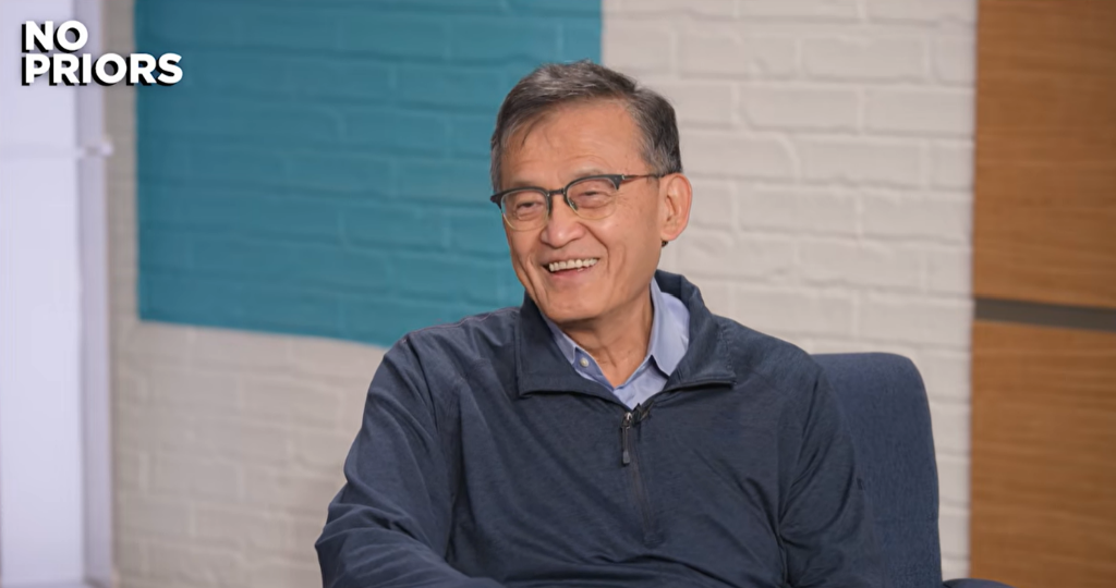
Intel CEO Lip-Bu Tan used his first appearance on the No Priors podcast to describe the transformation plan he is pursuing at Intel. His stated target is explicit: a “10x” return over five to ten years. He said Intel has already created roughly a sixfold return for shareholders over the past 14 months, but described that as only the beginning. In his view, Intel’s opportunity is not limited to the traditional PC client business; it also extends into data-center servers, edge computing, physical AI and agentic AI.
Tan, 66, is known as a veteran investor from Walden and as the former CEO of Cadence. He said he accepted the Intel role because the company is iconic and important to both the semiconductor ecosystem and the United States. After Cadence, he wanted to take on one more major challenge. During the interview, he also recalled an early episode in which President Donald Trump asked him to resign over a claimed conflict of interest. Tan said he explained that he was born in Malaysia, grew up in Singapore, graduated from MIT and had spent his life in the United States after that. He said Trump listened and gave him the opportunity to continue.
Balance sheet repair, product focus and direct engineering oversight
Tan framed Intel’s turnaround with his familiar “crawl, walk, run” approach. The first stage, he said, was cultural: changing accountability, accelerating decisions and reducing layers of bureaucracy. Coming from an engineering background, he decided from day one that all engineering teams would report directly to him so he could understand where problems existed and what needed to be corrected. He also emphasized listening to customers, simplifying the product line and building a clear roadmap and vision for the next five to ten years.
On the balance sheet, Tan said the situation was “quite bad” when he arrived. He welcomed the U.S. government becoming a major shareholder, saying he explained to Trump that infrastructure-level support from government could be seen in places such as Japan and Singapore. He also thanked Nvidia CEO Jensen Huang, whose $5 billion investment in Intel has, according to Tan, grown to $25 billion or more. SoftBank’s Masayoshi Son, with whom Tan had worked during his time on SoftBank’s board, also provided support. Tan said these steps helped stabilize Intel’s balance sheet.
Product demand has also shifted in Intel’s favor, according to Tan. He said the rise of agentic AI and inference workloads is lifting demand for CPUs. In training environments, the CPU-to-GPU ratio had previously been around one to eight; he now sees that moving toward one to four or even lower. Tan said AI model developers told him CPUs perform better in reinforcement learning and in coordinating the speed of many agents, which has made CPU demand in data-center servers stronger.
Foundry execution: trust, yield and cycle time
Intel’s foundry business has faced external doubts, but Tan said he decided to continue investing in it because supply-chain resilience matters to both the United States and the broader semiconductor industry. Large semiconductor companies, he argued, cannot depend entirely on suppliers concentrated in one or two geographies. He said Intel has already moved into 18A, described in the interview as a 1.4-nanometer-class process, and is planning paths toward 1 nanometer and 0.7 nanometer. As geometries shrink, manufacturing precision becomes increasingly demanding, and a single mistake can affect the outcome.
Tan said his core foundry metrics are yield, defect density and cycle time. Foundry work, in his words, is a service business and a business of trust: customers must trust Intel before they hand over wafers, and if yield fails to meet requirements, customers can leave after suffering revenue losses. He also pointed to the need for the right IP portfolio, including low-power IP for mobile customers. While discussing the competitive landscape, he said Intel respects TSMC and views it as a good partner, adding that the industry needs more capacity to serve customers. He also acknowledged that Intel still has a significant gap with TSMC and must stay humble.
Terafab with Elon Musk and the infrastructure gap behind AI
Tan also addressed the Terafab initiative with Elon Musk. He said he and Musk share a view that semiconductor infrastructure has not kept pace with AI growth in capacity, production efficiency and power efficiency. Musk’s robots and cars require large volumes of chips, so Musk decided to build his own fab. Intel will provide technology and process support to help accelerate production. Tan said he meets with Musk’s team every week and described the collaboration as energizing.
Tan said Musk brings an unconventional operating style and regularly asks why things must be done in the traditional way. One example he cited was a discussion about whether smoking could be allowed in certain areas of a cleanroom. Tan said he would not go that far, but some areas could be discussed, with the key being an open mindset and careful evaluation. When discussing the broader supply chain, Tan said AI’s effect on the world could be greater than the internet’s. He listed several bottlenecks: electricity constraints in some countries, the impact of helium on semiconductor manufacturing, memory shortages, and tight CPU and GPU supply that has pushed costs upward toward clients.
Advanced packaging, glass substrates and synthetic diamond wafers
As traditional process-node scaling approaches physical limits, Tan is looking to materials science and advanced packaging. He said Intel has 18A and is pushing 14A into production, while he can still see technical paths to 10 nanometers and 7 nanometers. That path, however, will become more expensive and more difficult. TSMC has CoWoS; Intel is pushing EMIB as its next-generation advanced packaging approach, with the focus on reaching customer-required yield in volume production.
On new materials, Tan said he has invested in gallium nitride, silicon carbide and indium phosphide companies, some of which have been acquired by large semiconductor companies such as ADI. He also invested in 3DGS, a glass substrate company, because he sees glass as a strong heat-dissipating insulating material. Intel has roughly 1,000 patents in modules, and Tan described the integration of substrates and modules as an important engineering problem. Intel has also announced advanced packaging manufacturing cooperation projects in India and New Mexico in the United States. In addition, Tan is studying synthetic diamond wafers and has invested in a diamond wafer company, citing diamond as another strong insulating material. “That is the spirit of engineers — you keep running into bottlenecks, and then you find a way to cross them or go around them,” he said.
Tan added that Moore’s Law is fundamentally about doubling transistor density, but power and cost do not automatically fall at the same rate. Performance can double, but area and cost do not necessarily improve in the same proportion unless new materials and new design methods are found. That is why he is increasing the hiring of materials science talent. Looking back, he said that 18 years ago many top-tier venture capitalists had little interest in semiconductors. Today, Nvidia has a market value of $5.3 trillion, Broadcom and TSMC are each around $2 trillion, Lisa Su’s AMD is close to $800 billion, and Intel is close to $600 billion. In Tan’s telling, semiconductors have again become foundational.
Investment discipline, AI-enabled organization and the 2030–2032 horizon
Tan also described his investing record and framework. He said he has been involved with 159 IPOs and 126 M&A exits, with more than 200 semiconductor investments, 38% of them in the United States. His starting question is always where the bottleneck is and what problem a company is solving. He invested in Cradle Semiconductor because interconnect became a bottleneck, and in Celestial AI because optical interconnect is increasingly important inside clusters. He also sees opportunities in EDA, AI and machine learning for design improvement, new materials and power management, including the loss that occurs when converting from 40V to 1V.
Reflecting on Cadence, where he spent nearly 15 years, Tan said one of the achievements he is most proud of was finding and mentoring his successor. Cadence is now bringing agentic AI into tools to improve efficiency. He said Sassine at Synopsys is working in a similar direction, supported by a $2 billion investment from Nvidia, while Synopsys has also acquired Ansys to expand into full-system design. Tan said large companies are active, but startups still have room to do more disruptive work and can eventually pursue IPOs or be acquired.
Within Intel, Tan is trying to move the company from an old-school organization dependent on spreadsheets into an AI-enabled company. He said the average age of the team is in the 40s to 50s, so he needs to bring in younger talent that understands workloads and frontier open-source models. He also said his son has become his teacher on AI and machine learning. On capital, Tan said infrastructure and capital-intensive businesses require access to large pools of funding, including government capital, sovereign wealth funds and major infrastructure funds, especially for AI factories and foundries.
Asked about the biggest misunderstanding investors have about Intel, Tan said many underestimate what is being built during the “crawl” stage. He is quietly rebuilding CPU architecture, GPU architecture and software architecture teams while improving IP, yield, defect density and cycle time on the foundry side. He said the market will begin to see Intel’s true potential around 2030 to 2032. He compared the challenge with his Cadence experience: from interim CEO through retirement, Cadence created about a 76x return for shareholders, and by the end of his executive chairman period, the return was around 85x. Intel is much larger and harder, he said, but his target remains a 10x return over five to ten years.
On the future location of compute, Tan said large-scale AI infrastructure buildout remains correct, and he sees constraints coming from supply rather than demand. His focus is on what large-scale applications will run on that infrastructure once it is built. He compared the process with the internet era, when Amazon and Netflix emerged as real applications while others disappeared or were acquired. Some workloads, including robotics and defense, fit better at the edge or on client devices, where assumptions about connectivity and on-device capability shape what can be done. For Intel, Tan wants to integrate XPU, advanced packaging and foundry capabilities to build customized chips for different workloads.