
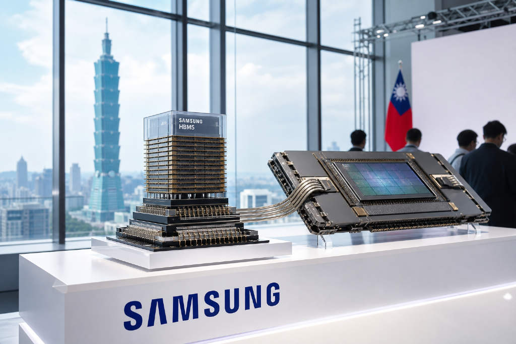
Samsung Electronics laid out a fresh memory tech plan, called CUBE, at the Memory Executive Summit before SEMICON Taiwan 2026. Choi Jang-seok, a vice president in Samsung’s memory product planning division, said the company will lean on 3D vertical stacking as the main path for getting past the physical limits of memory design. Samsung also showed a roadmap stretching from HBM5 to zHBM and zNAND-O, framing the whole thing around rising AI demand for memory capacity, bandwidth, and power efficiency.

CUBE centers on four design targets
CUBE stands for Capacity, Utilization, Bandwidth, and Efficiency. Samsung said the idea is to stop printed circuit board, or PCB, area from acting as a hard ceiling on memory capacity. The fix: stack chips upward, not outward, and grow capacity without making the PCB bigger.
During the presentation, Choi said, “The key to 3D is not simple stacking, but how fully each layer is used.” Put plainly, he said 3D design matters not because things are piled up, but because every layer has to earn its keep. The end goal, he said, is to fine-tune how logic and memory are placed across layers, reduce data-processing latency, and improve performance per watt.
TSV is the physical base of the stack
Samsung said through-silicon vias, or TSVs, are the physical base that makes 3D stacking work. Tiny copper vias run vertically through silicon dies. Samsung’s presentation said thousands of TSVs can link each layer, cutting chip-to-chip data travel from the millimeter range in conventional memory down to only tens of micrometers. Shorter trip. Faster signals. And a lot of data channels running in parallel.
Choi described the setup as a vertical data highway. Samsung said that is what lets HBM provide far higher bandwidth and better energy efficiency than standard DRAM in AI accelerators.
Three technology tracks: HBM5, zHBM and zNAND-O
HBM5
Samsung is using HBM4E as the yardstick for what comes next. It said HBM4E is now being sampled and tested by major customers. For HBM5, the company is aiming for 2x HBM4E performance, a 20% gain in performance per watt, and a 20% drop in thermal resistance.
zHBM
Samsung pitched zHBM as its boldest architectural move. The company said it first revealed the technology last month at FMS 2026 in California. The big shift is simple: instead of putting HBM beside a logic processor like a GPU or CPU, Samsung wants to stack HBM directly on top of it. That shrinks the data path between memory and compute units.
And Samsung said zHBM could also place customized IP blocks in an intermediate layer between the memory and the AI accelerator, giving customers more room for differentiated designs. The targets are steep: 8x the performance of HBM4E, up to 3x performance per watt, and a 75% to 90% cut in thermal resistance.
zNAND-O
zNAND-O is a 3D packaged storage product that stacks four or eight layers of V-NAND vertically with TSV. Samsung said it is built for the heavy storage needs of large language models, or LLMs. Against conventional NAND storage, the target is bit density 10x that of DRAM, plus read bandwidth and energy efficiency that are each 7x those of traditional NAND. Sampling is expected to start in 2028.
Samsung also pointed to current market share
The company tied the CUBE plan to the position it already holds in DRAM and NAND Flash. Citing Counterpoint Research, the report said Samsung had a 39% revenue share of the global DRAM market in the second quarter of 2026, ahead of SK hynix at 26% and Micron at 25%.
In NAND Flash, TrendForce data put Samsung at a 29.3% market share, again the highest in the industry. The report said strong demand for enterprise SSDs, pushed by AI servers, was the main driver of Samsung’s second-quarter NAND revenue.
Samsung said it intends to keep leaning on its technology base and manufacturing scale to meet demand across conventional memory and higher-value AI products such as HBM and enterprise SSDs.