BackzNAND-O

zNAND-O

Samsung Elect
2026-09-01 09:22:21

Samsung unveils CUBE 3D memory roadmap with HBM5, zHBM and zNAND-O for AI systems

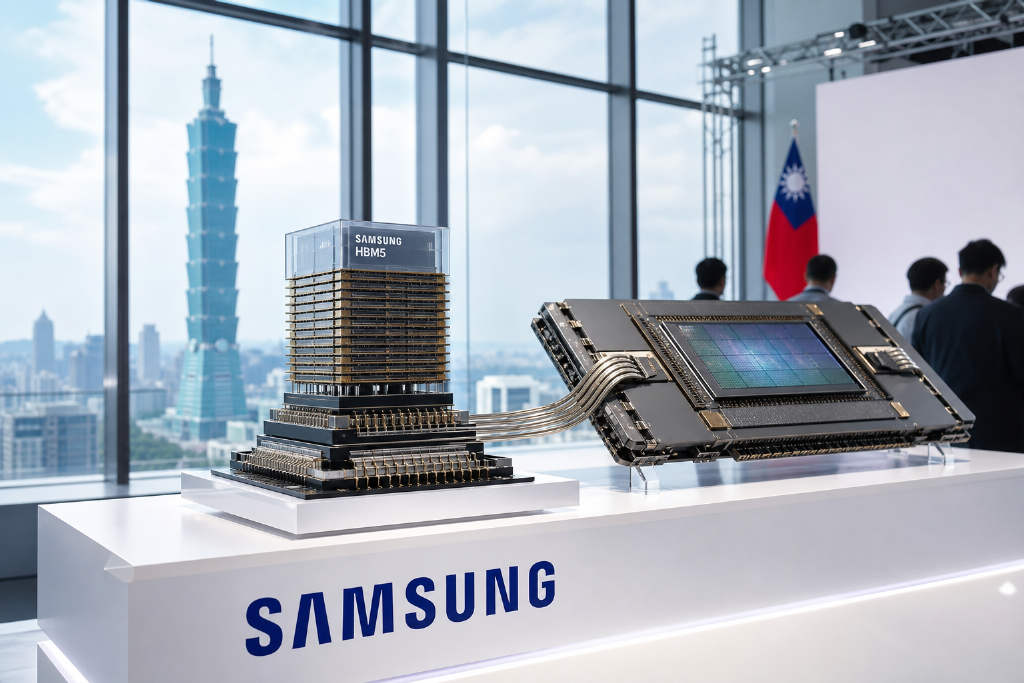
Samsung Electronics used the Memory Executive Summit ahead of SEMICON Taiwan 2026 to lay out a new memory strategy called CUBE, built around a 3D vertical stacking approach. Choi Jang-seok, a vice president in the company’s memory product planning division, said the plan is meant to address rising AI demand for capacity, bandwidth and power efficiency. CUBE stands for Capacity, Utilization, Bandwidth and Efficiency, and Samsung framed it as a way to move past printed circuit board size limits by stacking chips vertically. The company also detailed a three-part roadmap covering HBM5, zHBM and zNAND-O. Samsung said HBM5 is being developed with targets of 2x the performance of HBM4E, a 20% gain in performance per watt and a 20% reduction in thermal resistance. zHBM, first shown last month at FMS 2026 in California, would place HBM directly on top of logic processors such as GPUs or CPUs. Samsung said that design aims for 8x the performance of HBM4E, up to 3x performance per watt and a 75% to 90% drop in thermal resistance. zNAND-O, aimed at large language model storage needs, is designed to stack four or eight layers of V-NAND with TSV and is scheduled to begin sampling in 2028.

30
Samsung unveils CUBE 3D memory roadmap with HBM5, zHBM and zNAND-O for AI systems
FMS 2026
2026-08-07 11:37:04

FMS 2026 spotlights AI memory bottlenecks as SK hynix, Samsung and Kioxia push different storage paths

At FMS 2026 in Santa Clara, held from Aug. 4 to Aug. 6, storage vendors used the industry’s largest independent storage conference to show how AI system design is pushing memory and storage into a more central role. SK hynix and Sandisk introduced the first standard specification for High Bandwidth Flash, or HBF, through the Open Compute Project, with support for 8-high and 16-high stacks and capacity of up to 512GB per package. The product’s read bandwidth ranges from 0.4 TB/s to 3.0 TB/s, putting the top end into HBM4 territory, though it was presented as an added tier below HBM rather than a replacement for it. Samsung unveiled its V10 BV-NAND with more than 400 layers and said it was the industry’s first use of wafer bonding for that route, while also previewing zHBM and zNAND-O as concepts that have not entered mass production. Kioxia, for its part, introduced the CM10, described as the first enterprise SSD to combine PCIe 6.0, 332-layer BiCS10 and direct cold-plate liquid cooling. The report also said Samsung plans to raise monthly HBM output from about 170,000 wafers to about 250,000 wafers, with the target set for the end of 2026.

1670
FMS 2026 spotlights AI memory bottlenecks as SK hynix, Samsung and Kioxia push different storage paths
SpaceX
2026-08-05 02:32:00

SpaceX Bitcoin Losses, Coldcard Fallout and QUID Listings Lead a Packed Crypto Cycle

A heavy 24-hour news cycle in crypto and adjacent tech markets was led by SpaceX’s first earnings report as a public company, which showed $7.8 billion in second-quarter revenue, 18,712 BTC on its balance sheet, and roughly $540 million in unrealized losses after Bitcoin fell 33% in the quarter. Coldcard’s wallet security incident kept escalating as the company urged users to migrate funds, while Galaxy Digital’s Alex Thorn said at least 15 attackers have now been identified through victim reports and on-chain tracing. In South Korea, Upbit and Bithumb both moved to list QUID, while on-chain flows highlighted a new wallet buying CASHCAT, a 40x leveraged BTC short on Hyperliquid, HYPE unstaking, and another Strategy-linked BTC transfer. Elsewhere, U.S. crypto policy centered on the CLARITY Act and fresh political friction around Trump’s TRUMP meme coin, while institutions expanded tokenized finance, staking, and custody services through Wells Fargo, BNY Mellon, Circle, Dinari, and Cloudflare. Markets also tracked BIP-110 activation risk, lower Bitcoin implied volatility, Ethereum staking policy debate, major AI infrastructure deals, and a long list of company, macro, and semiconductor updates.

1660
SpaceX Bitcoin Losses, Coldcard Fallout and QUID Listings Lead a Packed Crypto Cycle
Samsung Elect
2026-08-05 00:15:00

Samsung unveils BV-NAND prototype and shows zHBM concept stacked above AI accelerators

Samsung Electronics introduced its V10 Bonding V-NAND, or BV-NAND, prototype at the Future of Memory and Storage conference in Santa Clara, California, held on Aug. 4 U.S. time, according to a report cited by PANews from Jin10. The company said the chip has more than 400 layers and uses a new wafer-bonding architecture designed to raise storage density and improve performance. Samsung said BV-NAND delivers about 58% higher storage density than its previous-generation V9 NAND, while also improving read, write, and input/output performance to meet rising demand from AI systems for higher-capacity and more energy-efficient storage. Samsung also presented what it described as the industry’s first zHBM and zNAND-O architecture concept models. The design vertically stacks memory units so more data can be stored in a smaller space. Unlike conventional HBM packaging, which places memory alongside an AI processor, Samsung’s zHBM stacks memory directly above an AI accelerator. The company said this shortens data transfer distance, increases bandwidth, improves energy efficiency, enables storage density of more than 10 times that of conventional HBM5 memory, and cuts thermal resistance by more than half.

990
Samsung unveils BV-NAND prototype and shows zHBM concept stacked above AI accelerators