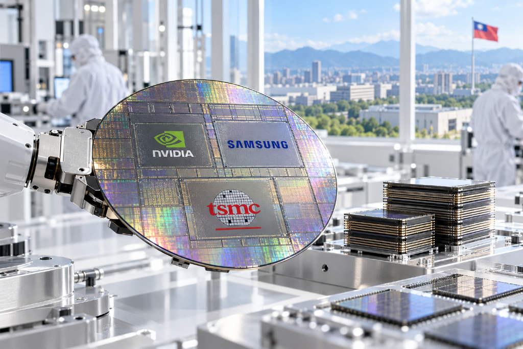
Samsung Electronics will use Taiwan Semiconductor Manufacturing Co. (TSMC)’s 3-nanometer process to produce base dies for Nvidia’s next generation of custom high-bandwidth memory, or HBM, chips, according to ChainCatcher. The move marks Samsung’s first collaboration with TSMC during the HBM manufacturing stage.
The report said Nvidia has asked Samsung, SK hynix and Micron Technology to manufacture NVHBM base dies with TSMC’s process and to adopt sixth-generation DRAM technology. At the same time, Samsung plans to keep producing standard HBM products on its own, along with custom products for other clients.
The update points to a more segmented production arrangement for Nvidia’s next HBM supply chain, with TSMC’s advanced process being used for the base die portion while Samsung maintains in-house production for standard HBM and some custom memory products.
Samsung Electronics will use Taiwan Semiconductor Manufacturing Co. (TSMC)’s 3-nanometer process to produce base dies for Nvidia’s next generation of custom high-bandwidth memory (HBM) chips, according to ChainCatcher.
The report said this is Samsung’s first cooperation with TSMC during the HBM manufacturing stage. Nvidia has asked Samsung, SK hynix and Micron Technology to make NVHBM base dies with TSMC’s process and to use sixth-generation DRAM technology.
Samsung plans to continue producing standard HBM on its own, as well as custom products for other clients.
This article was originally published by Bit.Fan. For more cryptocurrency news and market insights, visit www.bit.fan. Disclaimer:
The market information, project data, and third-party content displayed on this platform are for industry information sharing only and do not constitute any form of investment advice or return commitment.
Cryptocurrency trading carries high risks. Users should fully assess their risk tolerance and make independent decisions. All profits, losses, and legal responsibilities are borne by the users themselves.