


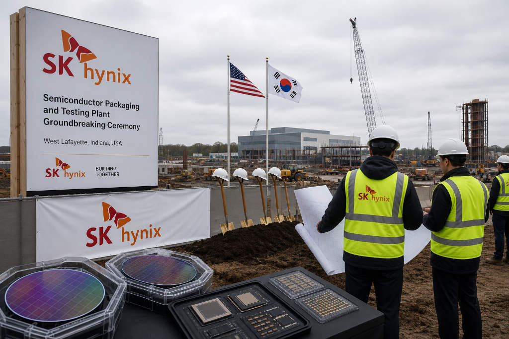
SK hynix held a groundbreaking ceremony on Aug. 27 in Indiana for an advanced packaging artificial intelligence wafer facility. The company said it plans to invest more than $4 billion in the project, which is designed to establish the first U.S. production base for high bandwidth memory, or HBM, and deepen semiconductor supply chain cooperation between South Korea and the United States.

Under the company’s plan, advanced wafers produced in South Korea will be shipped to Indiana, where they will go through advanced packaging and testing before being delivered to U.S. customers as products labeled made in America.
Timeline and operating plan for the Indiana facility
The plant will be located in West Lafayette, Indiana, with total investment set at more than $4 billion. SK hynix said the cleanroom is expected to begin operations in October 2028, and mass production of next-generation HBM is scheduled for the second half of 2029. The company expects the site to employ about 1,000 professional technical and operations staff.
In the cross-border production structure, domestic facilities in South Korea will manufacture advanced wafers, which will then be sent to the Indiana site for advanced packaging and testing before final delivery to local customers in the United States.
An advanced packaging R&D and testing platform will also be built next to the facility to support prototype manufacturing and performance verification for academic and industry partners.
Backed by U.S. chip policy support
The investment plan has received support under the U.S. CHIPS and Science Act. Political leaders and officials in Indiana also voiced support for the project.
U.S. Senator Todd Young said the project would deliver clear benefits for high-paying jobs and economic security. Indiana Governor Mike Braun said the arrival of the advanced packaging plant would help connect and upgrade the regional industrial chain, and that strengthening back-end semiconductor packaging capacity could improve the current semiconductor supply chain structure and raise the stability of advanced memory supply.
Local supply chain buildout and job creation
SK hynix said its Indiana expansion will support the localization of the AI industry supply chain in the United States. To keep the West Lafayette plant operating steadily, the company is evaluating the introduction of partners for materials, components, and equipment to strengthen the domestic AI hardware ecosystem.
According to the company’s internal estimate, construction and subsequent commercial operations will create about 7,000 direct and indirect jobs in the local area and across the United States. South Korea’s ambassador to the U.S. said the project goes beyond a standard investment, combining a memory production base with an R&D center and offering an example for talent development and cross-border industrial chain cooperation.
Purdue partnership and veteran employment channel
On the day of the groundbreaking ceremony, SK hynix signed a memorandum of understanding with Purdue University for research cooperation. The two sides will conduct joint research on system integration and advanced packaging technologies, including HBM, while also developing talent pipelines in the U.S. Midwest.
To broaden recruitment channels, SK Group said it would join an employment platform operated by the Korea Chamber of Commerce and Industry, or KCCI, and the Korea-U.S. Alliance Foundation, drawing on Indiana’s historical ties to the Korean War and offering career development opportunities for U.S. veterans who served in Korea.
SK hynix CEO Kwack Noh-jung said the United States has leading customers and research strengths, and that the Indiana facility will serve as an important gateway for delivering the first U.S.-made HBM products.