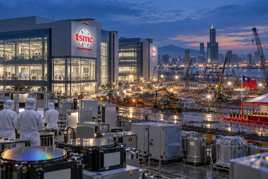
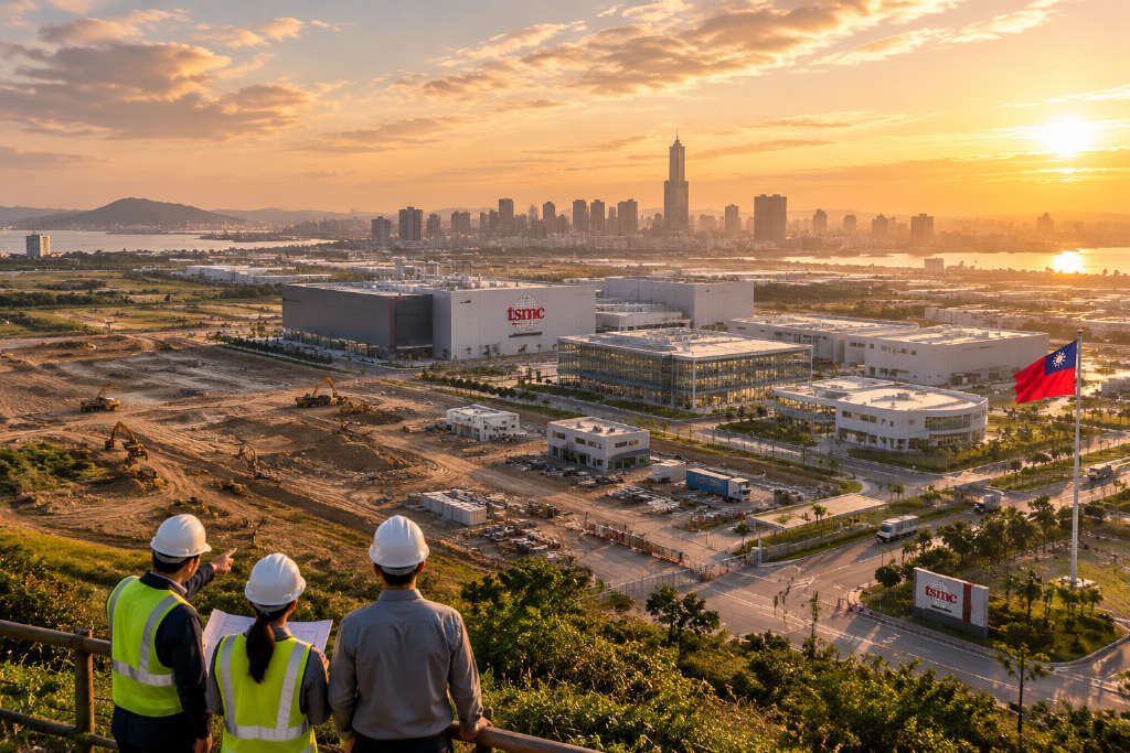
TSMC2026-09-21 03:46:36Kaohsiung’s Baipu semiconductor park breaks ground as TSMC plans advanced packaging validation siteConstruction on Kaohsiung’s Baipu Industrial Park began on Sept. 21, with the project positioned as a new node in southern Taiwan’s semiconductor supply chain. The park spans 88.73 hectares across Gangshan and Qiaotou, and about 25 hectares have been reserved for equipment makers and suppliers tied to advanced back-end semiconductor processes. Taiwan Semiconductor Manufacturing Co. (TSMC) plans to build two buildings there and set up a validation line so equipment and materials can complete integration testing before entering mass-production fabs. According to the report, this is the first time TSMC has placed an advanced packaging equipment validation platform outside its production system. The company will use a modular “mini-loop” process verification line, along with scaled-down cleanrooms and labs, to shorten testing cycles that currently can take more than a year. Kaohsiung city officials estimate the park could generate about NT$300 billion in annual output and create roughly 4,500 jobs once fully developed. The first batch of tenant signings, TSMC’s construction progress, and unresolved transport links are now among the main issues being watched by the industry.390
Kaohsiung2026-09-07 04:12:40TSMC and suppliers take 25 hectares in Kaohsiung advanced packaging hub as first phase fills upKaohsiung’s Baipu site is set to become Taiwan’s first advanced packaging industrial cluster, extending the city’s semiconductor footprint beyond wafer fabrication into packaging equipment, materials, R&D and verification. According to the report, the park covers 88.73 hectares, with about 53 hectares designated for industrial use. TSMC and key suppliers have secured 25 hectares, and the first round of tenant recruitment is already fully booked, with construction expected to begin in September this year. The planned setup goes beyond factory space. TSMC is expected to handle talent training and build a materials R&D lab, while the park will also include a wafer-level advanced packaging equipment and materials ecosystem zone, a TSMC verification and training center, and a third-party testing center operated by the Industrial Technology Research Institute. The goal is to link R&D, verification and mass production in one chain. TSMC Vice President of Advanced Packaging Technology and Service Ho Chun said CoWoS capacity is expected to post a compound annual growth rate of more than 80% through 2027. Local and central authorities are also rolling out incentives, including up to five years and NT$30 million in financing interest subsidies, along with rent, property tax and labor-related support.910
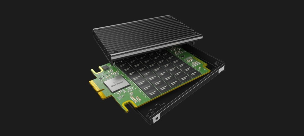
Winbond2026-08-07 07:02:35Winbond targets top global SLC NAND supplier spot by 2027 as DRAM shortages stretch onWinbond said DRAM supply will remain tight through 2027 and could get even tighter next year, while some customers are already discussing long-term supply agreements for 2029 and 2030. The company also outlined a plan to become the world’s largest SLC NAND supplier by 2027, backed by capacity expansion in Kaohsiung and a shift to 16nm. Analysts say the market is underestimating SLC demand tied to CMX and CXL-based AI server expansion.950