



After planar transistors, FinFETs and gate-all-around (GAA) nanosheets, the semiconductor industry is now treating complementary field-effect transistors, or CFETs, as the next major step in logic scaling. Over the past three years, Intel, Taiwan Semiconductor Manufacturing Co. (TSMC), Samsung and IBM Research have all shown silicon demonstrations that support the architecture’s feasibility, and several chipmakers see CFET as a key route beyond the 2 nm node and into the sub-1 nm era.
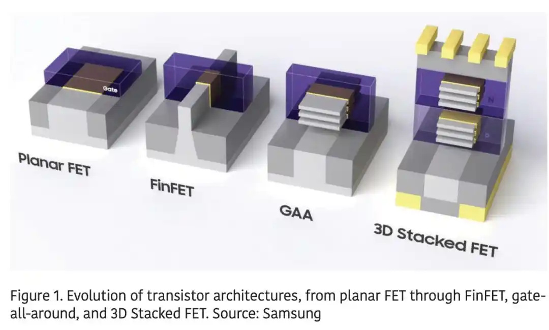
The idea is straightforward. Instead of placing n-type and p-type transistors side by side, CFET stacks them vertically. A standard CMOS inverter needs one NMOS and one PMOS device arranged next to each other, which consumes lateral wafer area. By stacking the two, CFET can in theory deliver the same logic function in about half the horizontal footprint.
The source notes that the industry has spent two decades extending Moore’s Law by repeatedly redesigning transistor structures. The path ran from planar devices to FinFETs and then to GAA nanosheets, with each transition opening roughly another decade of scaling room. Now that leading logic manufacturers are pushing nanosheet processes into production, CFET has become a central topic at the International Electron Devices Meeting, or IEDM, and the VLSI Symposium.
Two routes to the same stacked structure
There are two main ways to build CFETs, and the industry has not settled on one.
In monolithic integration, the bottom and top transistors are built on the same wafer through a continuous sequence of process steps. The lower device is completed first, then the channel material and gate stack for the upper device are formed above it. The flow is simpler as a whole, but the trade-off is severe: the finished bottom transistor must survive all the thermal and etch steps needed to build the upper one.
In sequential integration, the bottom and top transistors are fabricated on separate wafers, usually at different stages of the process and sometimes with different channel materials, before the wafers are bonded together. That eases the thermal budget problem, but it adds wafer bonding, alignment and extra lithography steps.
So far, the approaches shown by TSMC, Samsung and Intel have mostly used monolithic integration. IBM Research, by contrast, has built its roadmap around the sequential route.
IEDM 2023: CFET moves from slides to working devices
At IEDM in December 2023, CFET shifted from a presentation concept to functional hardware. Intel, Samsung and TSMC all presented data there, marking the first time the three companies showed CFET research at the same conference.
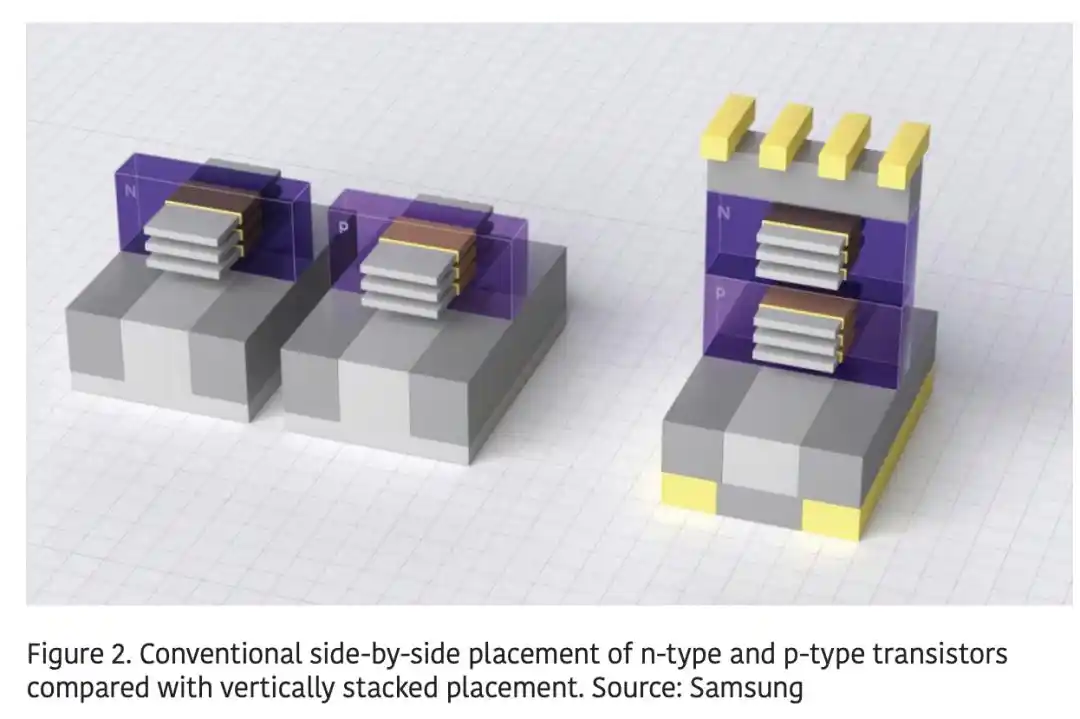
Intel presented a full inverter circuit rather than an isolated device. The circuit used a 60 nm contacted poly pitch (CPP), with three stacked nanosheets per device, up from two in earlier work, while device spacing was reduced from 50 nm to 30 nm. Intel also paired the demonstration with backside power delivery, connecting the lower transistor from beneath the wafer instead of routing both power and signal lines above the device. According to Intel, a fully scaled CFET inverter of this type could shrink to about half the area of an equivalent side-by-side CMOS inverter.
Samsung, working with its 3D stacked field-effect transistor, or 3DSFET, architecture, showed structures with a single nanosheet in each device pair at 45 nm and 48 nm CPP. The company also reported a process shift from wet chemical etching to dry etching when isolating the source and drain regions between stacked devices. Samsung said the change improved device yield by about 80% compared with its earlier method.
TSMC, in a 48 nm CPP design, used a high-germanium silicon-germanium (SiGe) layer so the isolation region between stacked nanosheets could be etched away earlier in the process, before the final nanowire release step. The source says that change in process order was intended to protect the isolation layer from later high-temperature steps. At the time, the industry estimate was that commercial CFET production was still seven to 10 years away, and later papers broadly supported that view.
IEDM 2024: from isolated devices to working logic gates
One year later, the technology had advanced from stand-alone devices to logic gates that could actually operate.
TSMC research and exploratory development director Sandy Liao presented what the company described as the first fully functional CFET inverter. It was built with a monolithic integration process and a 48 nm gate pitch. The devices showed balanced voltage transfer characteristics at voltages up to 1.2 V, and both the n-type and p-type devices posted subthreshold slopes of 74-76 mV/decade. The source describes those figures as strong for a first working circuit and already close to the targets needed for a production node.
Samsung and IBM Research jointly presented a variation on the standard CFET stack. Instead of using the same channel width for the top and bottom devices, the structure used a stair-step geometry: the bottom NFET had two wider nanosheet channels, while the top PFET had three narrower channels. IBM’s Chen Zhang said the stair-step geometry “alleviates the challenges associated with high-aspect-ratio processing by reducing the total stack height,” and also outperformed equal-width stacked structures within the same footprint. The wider bottom channel also gave process tools a more direct line of sight for forming contacts on the lower device, one of the hardest steps in CFET manufacturing.
Intel did not release new CFET data at IEDM 2024, despite having presented related work in the prior two years. The source says that absence drew some attention, but Intel’s later paper at the VLSI Symposium suggested a pause rather than a change in direction.
VLSI 2026: the work gets closer to manufacturing
By the 2026 Symposium on VLSI Technology and Circuits, both Intel and Samsung were presenting CFET results that looked more forward-leaning and more relevant to eventual production.
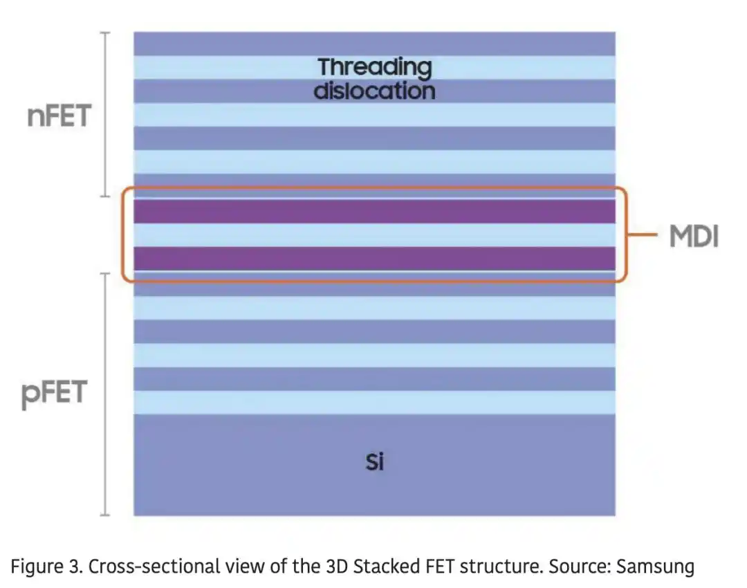
Intel’s paper described a CFET inverter built on a silicon substrate with a (110) crystal orientation. At a 45 nm gate pitch, the design integrated a 2×2 array of RibbonFET-style nanosheets and combined that with PowerVia backside power delivery and a backside direct-contact structure. It also used epi-to-epi vias to connect the stacked source and drain regions. The design placed the PMOS above the NMOS, the reverse of most published CFET work so far. Intel used a hybrid stack that combined (110) and (100) silicon to improve hole mobility in the upper PMOS device, while the two transistors were separated by an intermediate dielectric isolation layer less than 10 nm thick.
Samsung’s paper pushed scaling further with a 3DSFET structure that used three nanosheet channels in both the top and bottom devices at a 42 nm gate pitch. The source says this is the highest channel count yet reported for a stacked FET design. Samsung positioned it as a highly forward-looking CFET scaling option with near-term industrial manufacturing potential, not just a research demonstration.
IBM’s sequential route: Nanostack
While Intel, Samsung and TSMC have concentrated on monolithic integration, IBM Research has built its CFET roadmap around a sequential method it calls Nanostack. Rather than forming multiple transistor layers in one continuous process flow, IBM completes one layer first and then builds the next above it.
The main reason is thermal budget. In a monolithic structure, the lower transistor has to withstand every high-temperature step used to fabricate the upper transistor. IBM says those anneals can exceed 900°C and last for hours. In the sequential approach, each transistor layer is fabricated on its own wafer, the high-temperature steps are completed separately, and the wafers are bonded afterward, avoiding that thermal constraint.
IBM’s Nanostack design also does not place the upper and lower transistors in perfect vertical alignment. It uses an offset layout instead. IBM says that gives both the front side and back side of the transistors more direct contact points and simplifies interconnect routing, which would otherwise have to work around the full height of the stack.
IBM projects that, compared with current 2 nm-class process nodes, the technology could deliver about 50% higher performance, 70% better energy efficiency and a 40% reduction in area. The company also says the sequential method scales more readily than a single stacked-layer structure. By its estimate, a four-layer Nanostack device could cut circuit area by about another 40% compared with a two-layer version. IBM expects commercialization to take about six years from its latest published results.
The manufacturing problems are still severe
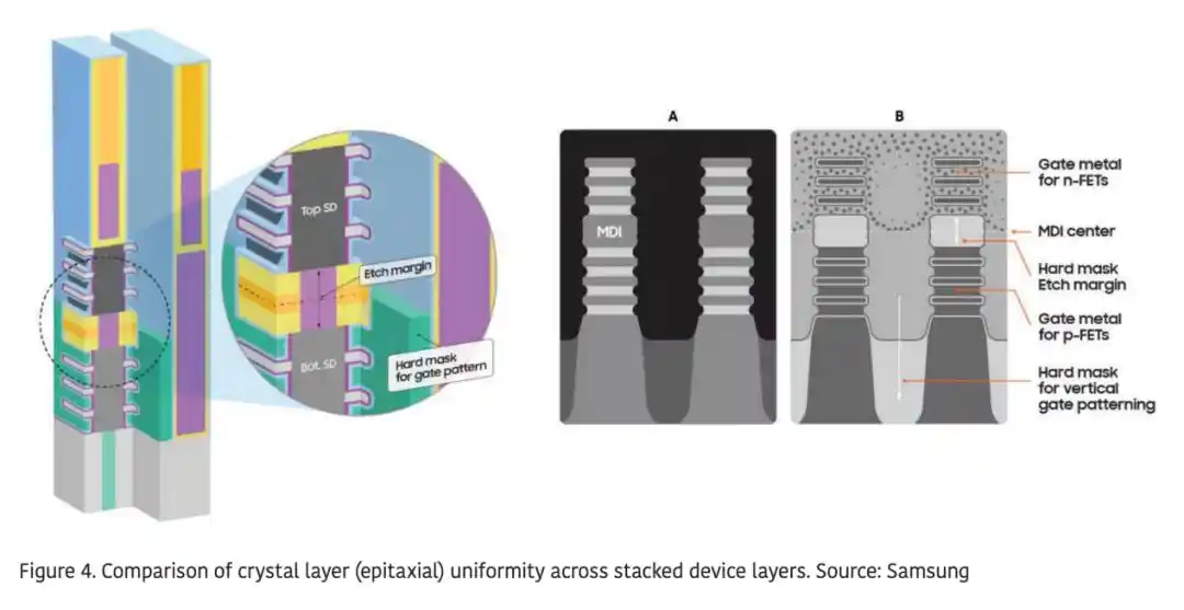
Even though the teams are pursuing different architectures, they are running into many of the same process problems. One of the hardest is how to connect the lower transistor sitting beneath the upper device, which in many cases can only be accessed from the backside after wafer thinning.
The papers discussed in the source are, in large part, different answers to that same problem. They include dry-etch isolation, offset layer structures, backside power vias and epi-to-epi interconnect vias. Another recurring issue is high-aspect-ratio fabrication. As transistor stacks get taller, engineers have to pattern and fill those structures without letting them collapse. Precise etch selectivity between the top and bottom channel materials is also critical, so processing one layer does not damage the other.
Equipment makers are seeing the same pattern. Lam Research describes the transition from FinFET to GAA and then to CFET as a path that depends more and more on atomic layer etch (ALE) and atomic layer deposition (ALD). Those processes can build spacers and other structural features one layer at a time. As devices become both taller and smaller in three dimensions, the source says the process flow must reach deeper into the structure and support 90-degree lateral processing.
Timelines still point to the early 2030s
Across forecasts published over the past three years, the timing has remained fairly stable. Most point to the early 2030s for CFET’s first appearance in volume logic chips, and some estimates extend that to 2032 depending on the source and how cautiously “volume production” is defined. That would put CFET about two full logic nodes behind current GAA technology.
By the industry’s usual pace, that leaves enough time for backside power delivery to mature and become mainstream. In fact, nearly every public CFET demonstration so far has combined the stacked transistor architecture with some form of backside contact or backside power routing.
What has changed since CFET was first proposed is not only the timeline but also the level of commitment behind it. Intel, TSMC, Samsung and IBM Research have now all shown functional CFET-based circuits at top conferences including IEDM and the VLSI Symposium, not just device concepts. Three have settled on monolithic integration, while IBM has committed to sequential integration. For a technology once treated as distant and mostly academic, the source says that is a clear sign of where advanced logic may head once the scaling room in GAA begins to run out.
The article was originally published by the WeChat account Semiconductor Industry Observation (ID: icbank) and credited to its editorial team.