
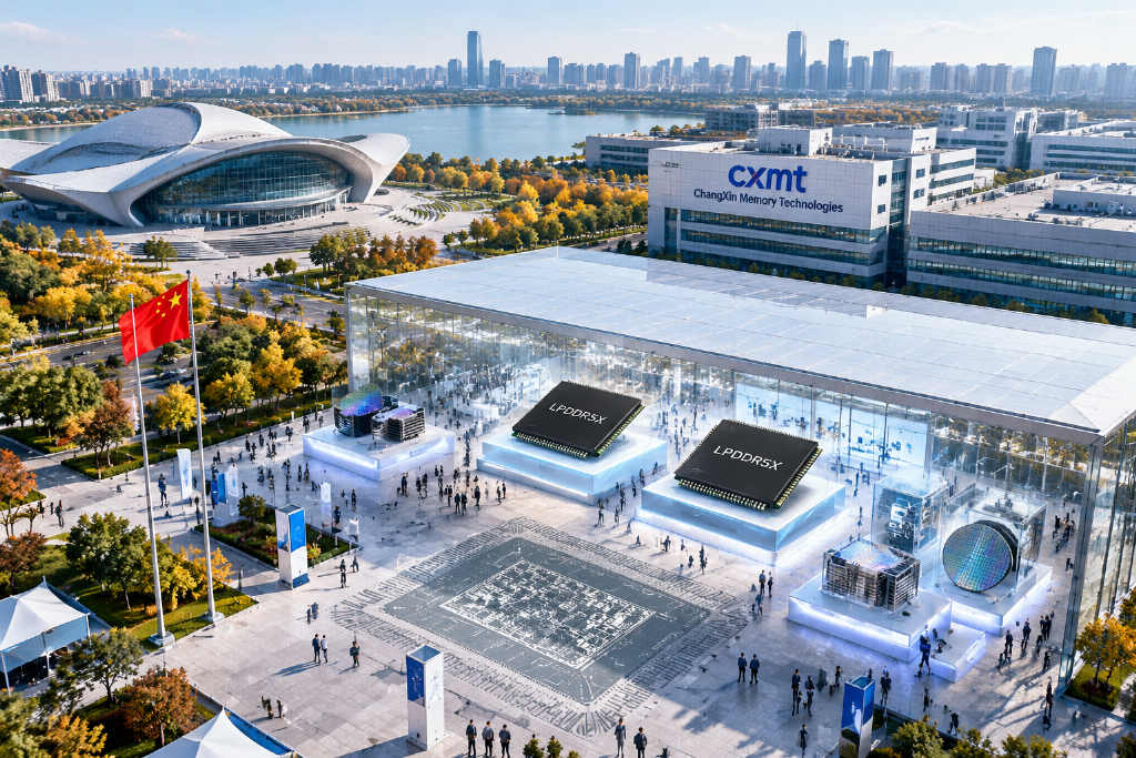
Changxin Memory Technologies announced on Sept. 20 at the 2026 World Manufacturing Convention that its fifth-generation DRAM technology platform, G5, has entered mass production. The company also showed two 24Gb LPDDR5X products based on the platform. The four figures it put forward were an 11.95 nm active-area half-pitch, a capacitor aspect ratio of 45:1, a 6,762 nm core functional area height, and at least a 50% increase in dies per wafer compared with the previous generation.
In the DRAM story, the weight of this announcement does not really sit in the words “fifth generation.” It sits in the route CXMT used to get there. The article says the company has pushed the process to roughly the industry’s 1c-class range without EUV. At the same time, it stresses that generational alignment is not the same thing as cost alignment, and each of the four headline figures comes with its own measurement context.
What the 11.95 nm figure actually refers to
The first point the article tries to clear up is one that can easily be blurred in coverage. The 11.95 nm figure refers to the “memory array active-area half-pitch,” a measurement taken from a specific structure in the array region. Samsung, SK hynix, and Micron, by contrast, usually describe their products with node labels such as “12 nm-class” or “11 nm-class.” Those are not the same yardstick, so they cannot be treated as direct equivalents. The article notes that overseas media including Seoul Economic Daily have already pointed this out.
Even on a conservative comparison, though, 11.95 nm still lands near the upper end of the most advanced mass-production range in the industry. The piece says SK hynix’s 1b node has an actual design dimension of roughly 12 to 13 nm and uses four EUV layers, while 1c shrinks to about 11 to 12 nm and uses five to six EUV layers. On that basis, CXMT’s number falls broadly on the 1c side.
The more important part is how it was achieved. Because of export controls, EUV lithography tools have still not entered the mainland China market, so CXMT has taken the DUV multi-patterning route. In the article’s description, one layer is split into four exposures and then overlaid, trading more process steps for higher resolution. The costs are straightforward: more mask layers, tighter overlay requirements, greater difficulty in controlling defect density, and longer process time per wafer. The industry has long questioned whether forcing advanced nodes with DUV can make economic sense. G5 now has to answer that question.
Paired with quadruple patterning is a set of modules migrated from logic manufacturing. HKMG, or high-k metal gate, had previously been used mainly in advanced logic, and the article says it has now been adapted into the DRAM flow to reduce the height of the core functional area. It also mentions a saddle-fin structure, low-k spacer bit lines, and interface engineering. Taken together, these changes suggest G5 is not a single-point breakthrough but a broader downward shift of the process stack.
The article also points to a digital twin system introduced on the R&D side, covering design, development, manufacturing, and maintenance. Its value, in the article’s framing, is not just whether the company can make the product once, but whether it can make it repeatedly and stably. For a manufacturer moving step by step through DRAM generations, that second challenge is no smaller than the first.
What “at least 50%” really means
The easiest figure to misread in the official presentation is the “+50%.”
The full wording cited in the article is that “the number of dies produced per wafer increased by at least 50% versus the fourth-generation platform, all converted to an 8Gb die basis.” Two qualifiers matter here. First, this is dies per wafer, or DPW, a theoretical count before defect screening. It is not the same as yield, which determines how much shippable output a fab can actually deliver. Second, CXMT did not disclose G5 yield levels or monthly output. The company’s own display board, according to the article, also noted that actual mass-production output may fluctuate within a normal range.
That distinction matters because DRAM manufacturing is a capital-heavy business. The article says a 12-inch DRAM fab requires investment on the order of tens of billions of dollars, and the number of usable chips cut from each wafer directly shapes unit cost. A 50% increase in DPW would, in theory, point to a meaningful drop in manufacturing cost per unit. But there is still a yield-ramp curve between design density and sellable capacity. The article is explicit on this point: the benefit will not be realized instantly, and it will not immediately hit global pricing.
There is another cost-side point in the piece. It says some industry estimates still put CXMT’s cost per bit above that of the three dominant players. The exact calculations may not be precise, but the direction is clear: process generation may have caught up, while cost structure has not. Saying that the company’s process level is comparable to the industry’s top mass-production nodes refers to the former, not the latter. That is why the article frames G5’s real commercial test in simple terms: not only whether CXMT can make it, but whether it can make it cheaply. The first is a technology proof. The second is what mass production really means.
A gap-filler in general DRAM, not a direct replacement
Shift the lens from process technology to business positioning, and CXMT’s place looks more nuanced than a standard catch-up story.
The article says the three global leaders are systematically steering capacity toward HBM and server DDR5. That has left structural gaps in more general product lines, including DDR4, standard DDR5, and lower-capacity LPDDR. CXMT is filling that space. Citing TrendForce data, the piece says the company held about 9.5% of global DRAM revenue in the second quarter of 2026, ranking fourth. The share is not large, but it makes CXMT the only player outside the top three that is still scaling volume, with room still rising.
Customer-side movement tells a similar story. Nubia’s NaviX Ultra uses CXMT’s 10,667 Mbps LPDDR5X, described in the article as the first large-scale commercial deployment of a domestic chip at that speed grade. Xiaomi’s 18 Fold is said to be the first to launch with CXMT LPDDR6, with a peak speed of 12,800 Mbps. The company’s half-year report also disclosed that LPDDR5 and LPDDR5X have entered the supply chains of Xiaomi and Transsion, while automotive-grade LPDDR5X has already entered mass production.
The article argues that flagship smartphones are sensitive at the same time to memory speed, power consumption, package size, and cost. Miss on any one of those and the part can be replaced. Passing into both of those customers, in that reading, means clearing a performance threshold rather than an emotional or symbolic one.
The LPDDR6 timing gets separate attention. CXMT announced mass production on Aug. 29, and the article describes it as the first LPDDR6 to land globally. SK hynix and Samsung are planning shipments in the second half of 2026, while Micron is expected to move to full commercialization in 2027. The article treats this as the first time a domestic DRAM maker has managed not to trail at product-generation launch, with G5 serving as the process base for follow-on supply.
The weak spots are also clear. G5 is centered on mobile LPDDR. Server DDR5 and HBM are not yet the main story. The article says CXMT’s gap with the three leaders in HBM is much larger than its gap in general-purpose DRAM. Its HBM3E is only at the stage of being “reportedly in pilot production,” and that has not been officially confirmed. The highest-value increment in AI computing still sits in HBM, which remains outside CXMT’s current reach. That leaves the company, for now, looking more like a gap-filler in general memory than a challenger in high-end compute memory.
The market is split on supply and demand
Views on the memory cycle are divided.
On the bullish side, Citi expects global DRAM demand to grow 30% in 2027 while supply rises 19%, then demand to grow 35% in 2028 against 22% supply growth. The shortfall, according to the article, would come from AI training demand for HBM and server DDR5.
On the more cautious side, Acer Chairman Jason Chen said on Sept. 19 that PC memory is no longer in short supply as mainland capacity comes online. He said some DDR4, LPDDR5, and DDR5-9600 part numbers are already seeing more sellers than buyers, and he expects the price uptrend could stop in the second half of next year.
The article says those two views do not necessarily conflict. Tightness is concentrated in HBM and high-speed server DDR5, while supply and demand in general-purpose parts are already loosening, with CXMT’s capacity expansion being one important source of that shift. That also means the company’s growth story remains tied to the memory cycle. Whether technology gains turn into profit depends on when prices retreat and by how much. DRAM is a strongly cyclical business, and in a downcycle the lowest-cost producers are the ones that survive best.
What to watch after G5
The article presents capital markets and technology progress as moving in step. On July 27, ChangXin Technology listed on Shanghai’s STAR Market at an issue price of 8.66 yuan, raising 57.9 billion yuan in what the article calls the largest IPO in the board’s history. Its market capitalization at the first close was about 3.28 trillion yuan, ranking first in the A-share market, and later briefly exceeded 4 trillion yuan. For the first half of 2026, the company reported revenue of 150.31 billion yuan, up 873.64% year over year, and net profit attributable to shareholders of 77.605 billion yuan, enough to erase all accumulated losses since its founding. In that context, the launch of G5 is framed as a moment when financial delivery and technology narrative arrived together.
The article ends by narrowing the watch list to three items rather than the “fifth-generation” label itself: the actual slope of the yield ramp, the speed at which cost per bit converges toward the three leaders, and when HBM moves from rumor to product. The first two will decide whether the route around EUV can keep working. The third will decide whether CXMT can move from being a participant in general memory to becoming a participant in the computing era.
This article was sourced from the WeChat public account Xinshiye and written by Domi.