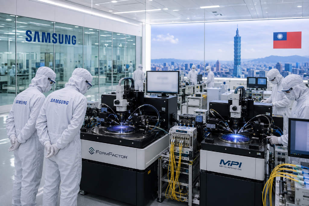
Samsung Electronics is using probe stations from U.S.-based FormFactor and Taiwan-based MPI to test silicon photonic integrated circuit, or PIC, wafers, according to a report by Korean semiconductor outlet The Elec cited by BlockBeats on Sept. 7. The company aims to complete its own internal PIC evaluation within the year.
The report said both FormFactor and MPI have already passed equipment verification tied to Taiwan Semiconductor Manufacturing Co.'s co-packaged optics, or CPO, and silicon photonics testing workflows. Samsung is using the same basic testing setup to examine optoelectronic properties of PIC wafers across wavelength and frequency domains, checking whether optical devices perform signal transmission and electro-optic conversion as intended.
Samsung had previously relied on outside institutions including Belgium-based imec for PIC wafer verification. It is now building its own testing environment and conducting repeat evaluations. The company is also preparing customer evaluations and has said related projects will enter mass production starting in the second half of this year. The report added that Samsung plans to launch silicon photonics foundry services in 2027, offering optical device process technology, device libraries and PDKs, while also developing optical engines that combine EIC and PIC for future CPO use in products beyond network switches, including GPUs and CPUs.
Samsung Electronics is using probe stations from U.S. company FormFactor and Taiwan-based MPI to test silicon photonic integrated circuit (PIC) wafers, and plans to complete its own in-house PIC evaluation within this year, according to Korean semiconductor publication The Elec.
The report, cited by BlockBeats on Sept. 7, said FormFactor and MPI have both passed equipment verification related to Taiwan Semiconductor Manufacturing Co.'s co-packaged optics (CPO) and silicon photonics testing. Samsung is adopting the same underlying testing infrastructure used by TSMC to run wavelength-domain and frequency-domain optoelectronic tests on PIC wafers. The goal is to verify whether optical devices are transmitting optical signals and carrying out electro-optic conversion in line with their design.
Samsung had previously commissioned external organizations including Belgium-based imec to verify PIC wafers. It is now building its own testing environment and carrying out repeat evaluations.
The company also plans to move ahead with customer evaluations, and has said related projects will begin mass production in the second half of this year.
The report added that Samsung plans to start silicon photonics foundry services in 2027, offering optical device process technology, device libraries and process design kits, or PDKs. At the same time, it is developing optical engines that combine electronic integrated circuits (EIC) and PICs, with plans to expand future CPO applications from network switches to products such as GPUs and CPUs.
This article was originally published by Bit.Fan. For more cryptocurrency news and market insights, visit www.bit.fan. Disclaimer:
The market information, project data, and third-party content displayed on this platform are for industry information sharing only and do not constitute any form of investment advice or return commitment.
Cryptocurrency trading carries high risks. Users should fully assess their risk tolerance and make independent decisions. All profits, losses, and legal responsibilities are borne by the users themselves.