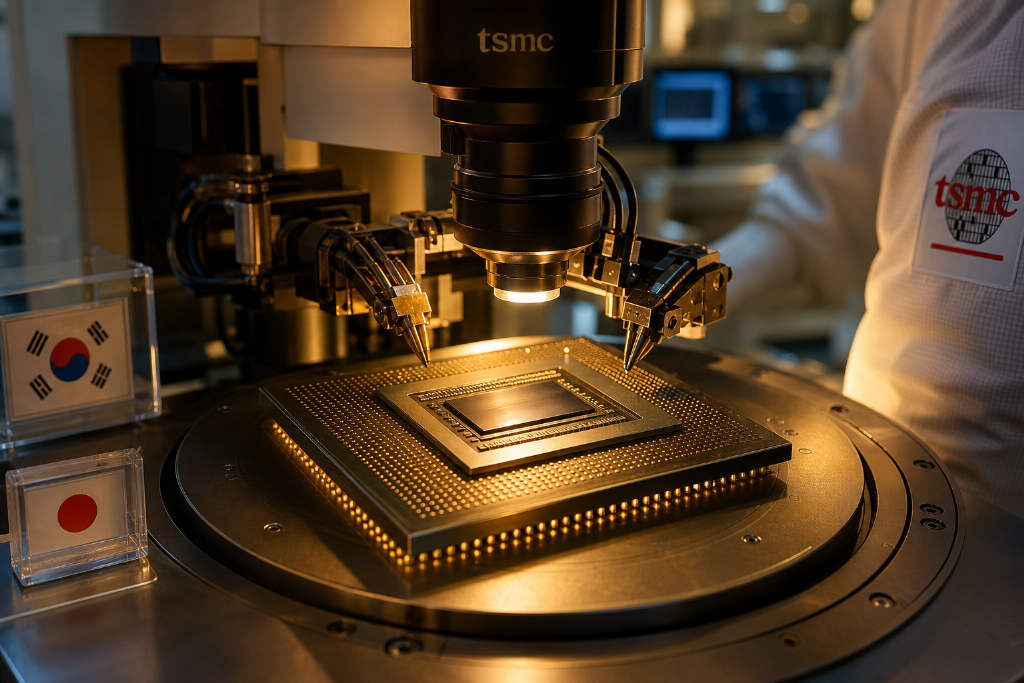
TSMC expects to keep using conventional microbumps, not hybrid bonding, to link high-bandwidth memory with AI accelerators in advanced packaging over the near term, according to materials industry sources on Sept. 2. Finer-pitch microbumps are likely to remain in use through late HBM4 and into early HBM5, reflecting material development lead times. TSMC has asked materials and equipment partners to develop bonding and underfill solutions for roughly 5μm bumps, and Korean and Japanese suppliers have started work. Volume production for 5μm-class bumps is expected in the second half of 2028. Today's HBM3E bumps are about 15–25μm high, while HBM4 is approaching around 10μm. Japanese materials suppliers have said it is difficult to guarantee quality below 15μm. The push for shorter, finer bumps comes from height limits on HBM stacks and the need for denser interconnects. JEDEC caps HBM stack height at 775μm. In TSMC's CoWoS flow, GPU dies and preassembled HBM stacks attach to a silicon interposer via microbumps, while SK hynix and Samsung Electronics build the 16-layer DRAM die stacks in HBM packages. First- and second-generation HBM relied on larger solder bumps; microbumps became mainstream around the HBM3 generation. SK hynix uses MR-MUF, and Samsung Electronics uses TC-NCF. Hybrid bonding can make interconnects thinner and denser by directly bonding copper pads, and TSMC has applied it to logic stacking on its SoIC platform, but HBM still connects to the interposer through microbumps.
TSMC expects to stick with traditional microbumps for the packaging connections between HBM and AI accelerators for the near term, rather than move to hybrid bonding, materials industry sources said Sept. 2. Finer-pitch microbumps are expected to stay in use through the late stages of HBM4 and the early stages of HBM5, given how long materials development can take.
TSMC has asked materials and equipment partners to develop bonding and underfill solutions for bumps around the 5μm level. Suppliers in South Korea and Japan have started development, and mass production of 5μm-class bumps is expected to begin in the second half of 2028.
Bump heights have been moving down. HBM3E, the third-generation extended HBM, uses bump heights of about 15–25μm. HBM4 is heading toward roughly 10μm. Japanese materials suppliers have previously said that quality below 15μm is hard to guarantee.
Shorter and finer bumps are needed because HBM stacks face strict height limits and require denser interconnects. JEDEC puts the maximum HBM stack height at 775μm.
Inside TSMC's advanced CoWoS packaging, a GPU and HBM stacks pre-assembled by memory suppliers are attached to a silicon interposer through microbumps. SK hynix and Samsung Electronics handle the 16-layer DRAM die stacking within HBM packages. First- and second-generation HBM used larger solder bumps, while microbumps became the mainstream around the HBM3 generation. SK hynix uses its MR-MUF process; Samsung Electronics uses TC-NCF.
Hybrid bonding, which directly connects copper pads, enables thinner and denser interconnects. TSMC has already used it for logic stacking on its SoIC platform, but the HBM-to-interposer connection remains on microbumps.
This article was originally published by Bit.Fan. For more cryptocurrency news and market insights, visit www.bit.fan. Disclaimer:
The market information, project data, and third-party content displayed on this platform are for industry information sharing only and do not constitute any form of investment advice or return commitment.
Cryptocurrency trading carries high risks. Users should fully assess their risk tolerance and make independent decisions. All profits, losses, and legal responsibilities are borne by the users themselves.