BackMR-MUF

MR-MUF

SK hynix
2026-09-07 00:12:13

SK hynix speeds up 1c DRAM ramp, with Q4 share seen topping Samsung

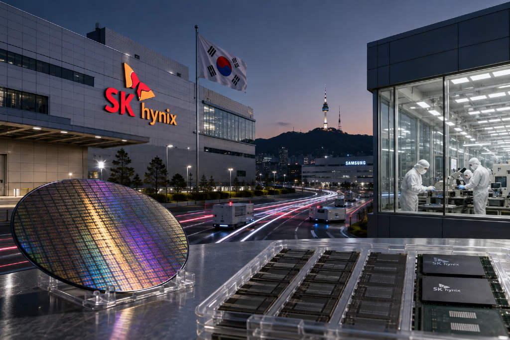
SK hynix is accelerating the production mix shift toward its sixth-generation 10nm-class 1c DRAM, according to a Sept. 7 report by The Chosun Daily cited by ChainCatcher. Industry data showed the company’s 1c DRAM mix rising from about 10% in the first quarter to roughly 13% in the second quarter, with forecasts of around 24% in the third quarter and 34% in the fourth quarter. By the first quarter of next year, the share could reach about 35%, surpassing 1b DRAM at roughly 33% for the first time and becoming the company’s leading process node. The report also said SK hynix may overtake Samsung Electronics in 1c mix by the fourth quarter, after trailing both Samsung and Micron at the end of the second quarter. The company has said 1c-based DRAM supply began in earnest in the second quarter, and expects bit growth in the second half to exceed the first half as HBM4 volumes rise and shipments of 1c commodity DRAM increase.
120
SK hynix speeds up 1c DRAM ramp, with Q4 share seen topping Samsung
TSMC
2026-09-02 06:56:05

TSMC Sticks With Microbumps for HBM Packaging; 5μm-Class Output Seen in 2H 2028

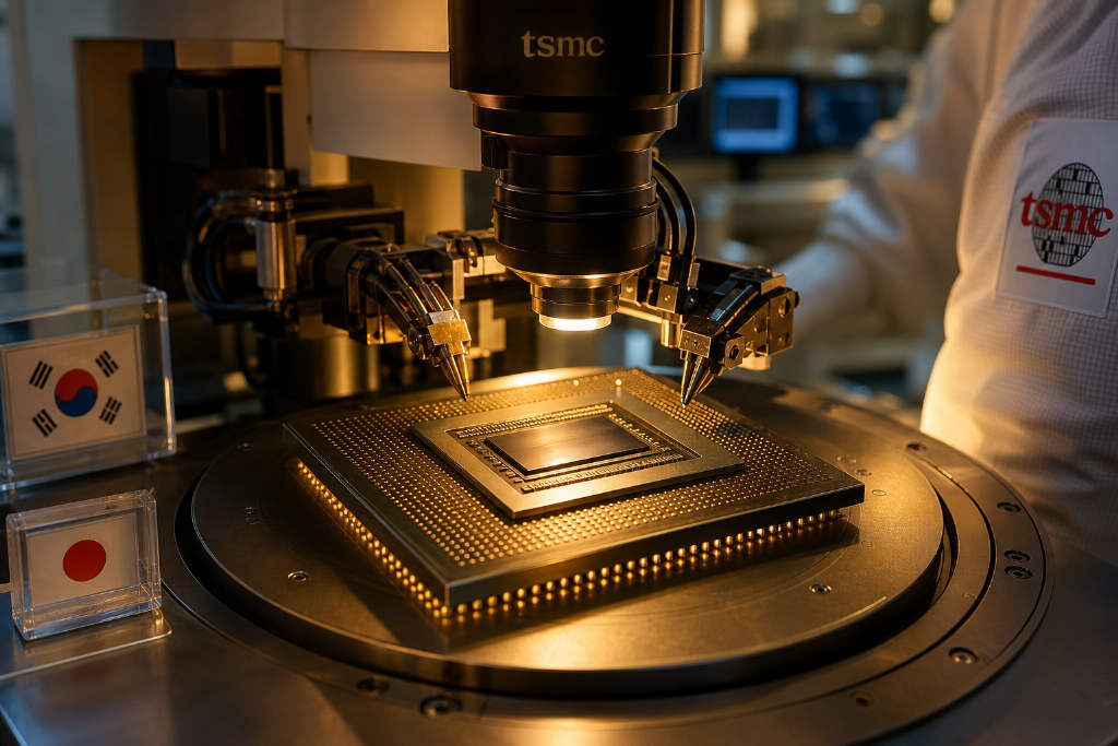
TSMC expects to keep using conventional microbumps, not hybrid bonding, to link high-bandwidth memory with AI accelerators in advanced packaging over the near term, according to materials industry sources on Sept. 2. Finer-pitch microbumps are likely to remain in use through late HBM4 and into early HBM5, reflecting material development lead times. TSMC has asked materials and equipment partners to develop bonding and underfill solutions for roughly 5μm bumps, and Korean and Japanese suppliers have started work. Volume production for 5μm-class bumps is expected in the second half of 2028. Today's HBM3E bumps are about 15–25μm high, while HBM4 is approaching around 10μm. Japanese materials suppliers have said it is difficult to guarantee quality below 15μm. The push for shorter, finer bumps comes from height limits on HBM stacks and the need for denser interconnects. JEDEC caps HBM stack height at 775μm. In TSMC's CoWoS flow, GPU dies and preassembled HBM stacks attach to a silicon interposer via microbumps, while SK hynix and Samsung Electronics build the 16-layer DRAM die stacks in HBM packages. First- and second-generation HBM relied on larger solder bumps; microbumps became mainstream around the HBM3 generation. SK hynix uses MR-MUF, and Samsung Electronics uses TC-NCF. Hybrid bonding can make interconnects thinner and denser by directly bonding copper pads, and TSMC has applied it to logic stacking on its SoIC platform, but HBM still connects to the interposer through microbumps.

150
TSMC Sticks With Microbumps for HBM Packaging; 5μm-Class Output Seen in 2H 2028
HBM
2026-08-25 01:13:19

HBM Splits Into Diverging Paths as Samsung Pushes zHBM and SK Hynix Targets Taller Stacks

High Bandwidth Memory is no longer being framed as a standalone memory problem. At Hot Chips 2026, Samsung and SK Hynix both argued that GPUs, memory, foundry processes and packaging now have to be designed as one system, but the two companies outlined sharply different routes. Samsung is trying to turn the HBM base die from a passive bridge into an active logic layer, moving the memory controller off the GPU, adding memory expansion and selective compute to the base die, and ultimately aiming for zHBM, a structure that vertically stacks DRAM directly on top of compute silicon. Samsung said that approach could free up 5% to 10% of GPU area, lift performance by 10% to 20%, cut DRAM power by about 70%, and deliver more than 2.3x the bandwidth of HBM4E. SK Hynix, by contrast, is concentrating on higher stack counts and the thermal and warpage penalties that come with them. The company said 12-high HBM4 is in production and 16-high parts are in customer validation, while hybrid bonding remains in R&D for 20-high and above. It also presented iHBM, a thermal path built into the hottest region of the stack. Micron took a third angle, arguing that the AI memory wall is widening as accelerator compute rises faster than attached-memory bandwidth, forcing increasingly difficult trade-offs across bandwidth, capacity, packaging complexity, heat and reliability.

1010
HBM Splits Into Diverging Paths as Samsung Pushes zHBM and SK Hynix Targets Taller Stacks
SK Hynix
2026-07-11 04:02:19

SK Hynix raises $26.5 billion in Nasdaq debut, ranking as the world’s second-largest IPO

SK Hynix made its Nasdaq debut on July 10 Beijing time, with its shares rising more than 18% intraday and its market capitalization closing at $1.22 trillion, or roughly RMB 8.3 trillion. The company raised $26.5 billion through an American depositary receipt offering, setting what the source described as the largest U.S. IPO ever by a foreign company and placing it behind only SpaceX, which went public last month, in the global all-time IPO rankings. The listing caps a long turnaround story. Founded in 1983 as Hyundai Electronics, the business expanded through its acquisition of LG Semiconductor in 1999 but later fell into distress as memory prices collapsed and debt mounted. Its memory operations were spun off in 2001 into Hynix Semiconductor, which remained under creditor control until SK Group acquired it in 2011. The company was renamed SK Hynix in 2012. Its long bet on high bandwidth memory, or HBM, became central to that recovery. After years of investment, SK Hynix became a key supplier of HBM3 for Nvidia’s H100 chips following the AI surge that accelerated after ChatGPT emerged in 2022. The report says the company now holds 58% of the global HBM market. It also points to strong profit margins, a sharp share-price gain, and rising investor attention toward Chinese memory makers such as CXMT, which is scheduled to open its share subscription on July 16.

1180
SK Hynix raises $26.5 billion in Nasdaq debut, ranking as the world’s second-largest IPO