4 nm

AMEC
2026-08-31 12:11:14

AMEC’s rise in etching tools puts China chip equipment makers under a brighter global spotlight

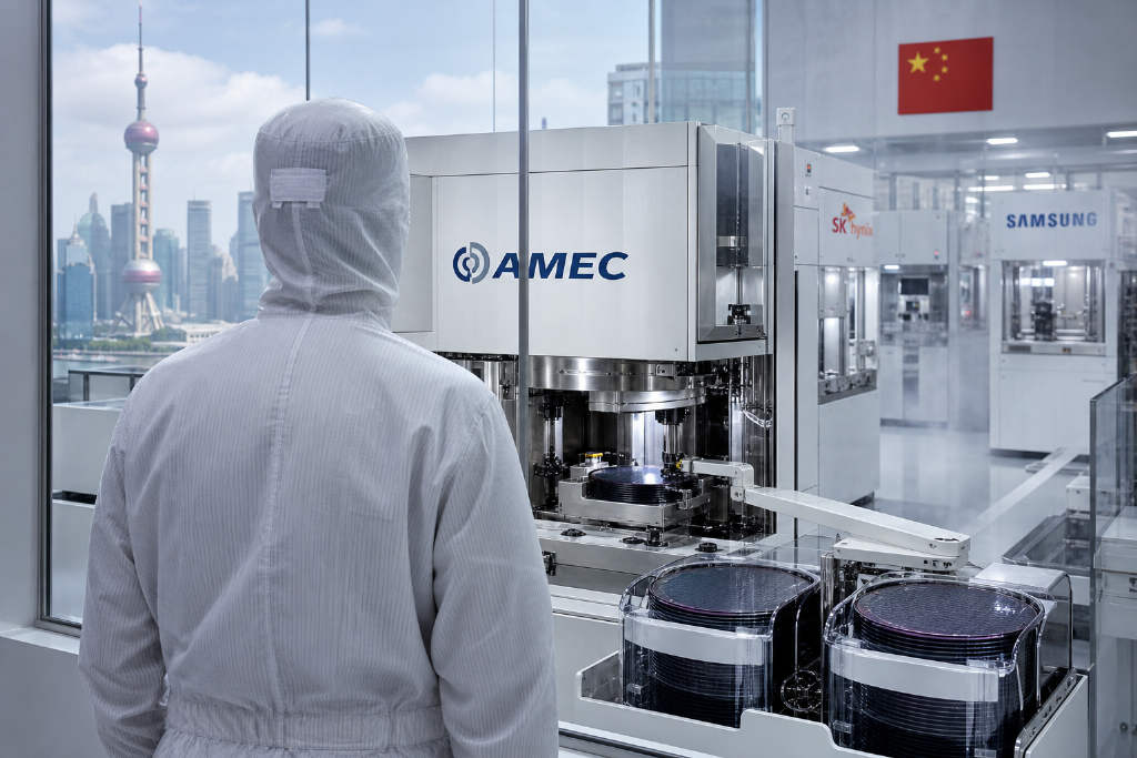
A long-form report carried by MarsBit and credited to WeChat account HSTL8888 traces how Advanced Micro-Fabrication Equipment Inc. China, or AMEC, moved from a startup backed by local government funding in Shanghai to a supplier validated by Taiwan Semiconductor Manufacturing Co. The piece opens with a Reuters report from early August saying Samsung Electronics and SK Hynix were evaluating AMEC chipmaking tools for use in their fabs in China, and that testing of the company’s etching tools may have started about two years ago. Samsung later denied it had ever considered the move, while SK Hynix declined to comment. The report then broadens into a history of China’s semiconductor equipment industry, covering AMEC, Piotech-related deposition efforts, Hwatsing for CMP, Skyverse for wafer inspection, ACM Research Shanghai for cleaning tools, and NAURA as a platform-style equipment company built through acquisitions. It argues that tightening U.S. export controls, support from domestic fabs such as Semiconductor Manufacturing International Corp. and funding through the National Integrated Circuit Industry Investment Fund together accelerated localization. Citing industry and official figures, the article says China’s overall localization rate in semiconductor equipment rose from under 5% to about 20% by 2025, while major foundries kept capacity utilization above 90% in the first seven months of this year.

920
AMEC’s rise in etching tools puts China chip equipment makers under a brighter global spotlight
HBM
2026-08-25 01:13:19

HBM Splits Into Diverging Paths as Samsung Pushes zHBM and SK Hynix Targets Taller Stacks

High Bandwidth Memory is no longer being framed as a standalone memory problem. At Hot Chips 2026, Samsung and SK Hynix both argued that GPUs, memory, foundry processes and packaging now have to be designed as one system, but the two companies outlined sharply different routes. Samsung is trying to turn the HBM base die from a passive bridge into an active logic layer, moving the memory controller off the GPU, adding memory expansion and selective compute to the base die, and ultimately aiming for zHBM, a structure that vertically stacks DRAM directly on top of compute silicon. Samsung said that approach could free up 5% to 10% of GPU area, lift performance by 10% to 20%, cut DRAM power by about 70%, and deliver more than 2.3x the bandwidth of HBM4E. SK Hynix, by contrast, is concentrating on higher stack counts and the thermal and warpage penalties that come with them. The company said 12-high HBM4 is in production and 16-high parts are in customer validation, while hybrid bonding remains in R&D for 20-high and above. It also presented iHBM, a thermal path built into the hottest region of the stack. Micron took a third angle, arguing that the AI memory wall is widening as accelerator compute rises faster than attached-memory bandwidth, forcing increasingly difficult trade-offs across bandwidth, capacity, packaging complexity, heat and reliability.

1890
HBM Splits Into Diverging Paths as Samsung Pushes zHBM and SK Hynix Targets Taller Stacks
Etched
2026-08-19 03:04:07

Etched Delivers First Inference Rack as New Funding Lifts Valuation to $21 Billion

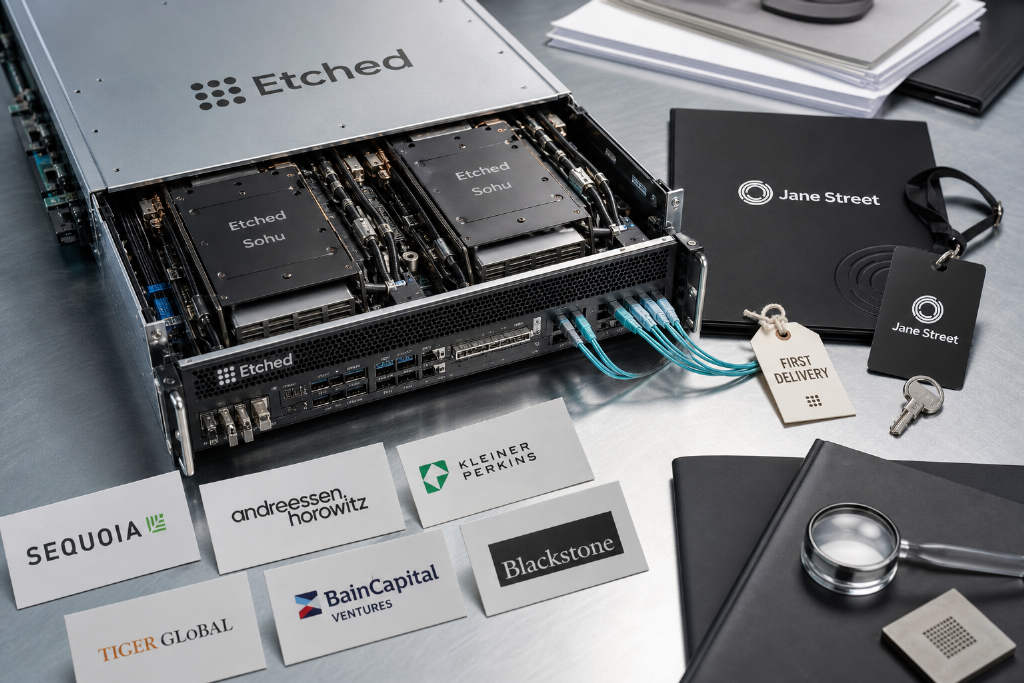
AI chip startup Etched said on August 18 that it raised $700 million at a post-money valuation of $21 billion, with quantitative trading firm Jane Street leading the round. The company also said it delivered its first inference rack to Jane Street on the same day, making the lead investor the only publicly confirmed customer to have received Etched hardware so far. Existing and new backers named in the announcement include Sequoia, Andreessen Horowitz, Kleiner Perkins, Tiger Global, Bain Capital Ventures, Blackstone, and Peter Thiel. Founded in 2022 by Harvard dropouts Gavin Uberti, Chris Zhu, and Robert Wachen, Etched is building Sohu, an ASIC designed specifically for Transformer inference and manufactured on TSMC’s 4 nm process. The company says an eight-Sohu server can generate more than 500,000 tokens per second on Llama 70B, compared with roughly 23,000 tokens per second for an eight-H100 setup. It has also shifted its pitch in 2026 from custom chips for specific large models to a broader claim that its system can run any frontier model. The valuation jump has come with scrutiny. Critics including tinygrad founder George Hotz and blogger Zach have questioned Etched’s marketing, the absence of independent third-party production benchmarking, and changes in its product narrative. Jane Street said it tested the chips and was satisfied with the early results, but the gap between a first delivered rack and proven large-scale commercialization remains central to the debate around Etched.

1280
Etched Delivers First Inference Rack as New Funding Lifts Valuation to $21 Billion
TSMC
2026-08-10 03:22:03

Longtan science park expansion restarts as TSMC signals interest in 1.4 nm fabs

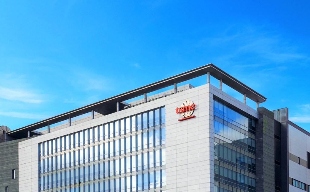
The long-delayed third-phase expansion of the Longtan Science Park has been revived after more than two years of setbacks tied to land expropriation disputes. According to ABMedia, citing a Liberty Times report, local sentiment in Longtan shifted after residents saw the economic spillover created by Taiwan Semiconductor Manufacturing Co. (TSMC) plants in southern Taiwan, including Tainan, Kaohsiung, and Chiayi. Supply chain sources said TSMC is planning three facilities for the site: two 1.4 nm wafer fabs and one panel-level packaging, or PLP, plant. The project was originally designed to cover 158.59 hectares, with 88% of the land privately owned, triggering strong opposition and organized protests. TSMC later announced on Oct. 17, 2023 that it would abandon its Longtan plant plan. Since then, the project scope has been revised several times, first to 89.63 hectares in 2024 and later to 104.19 hectares, of which about 46 hectares are designated for industrial use. Taiwan’s National Science and Technology Council said the expansion plan passed review by the Science Park Review Committee in May and was submitted to the Executive Yuan in June. Under the current timetable, land acquisition is targeted for completion by the end of 2029, with public infrastructure construction scheduled to begin in 2030.

2310
Longtan science park expansion restarts as TSMC signals interest in 1.4 nm fabs
ASML
2026-07-15 14:54:59

ASML lifts guidance and maps out 2027-2028 capacity expansion as Wall Street turns broadly bullish

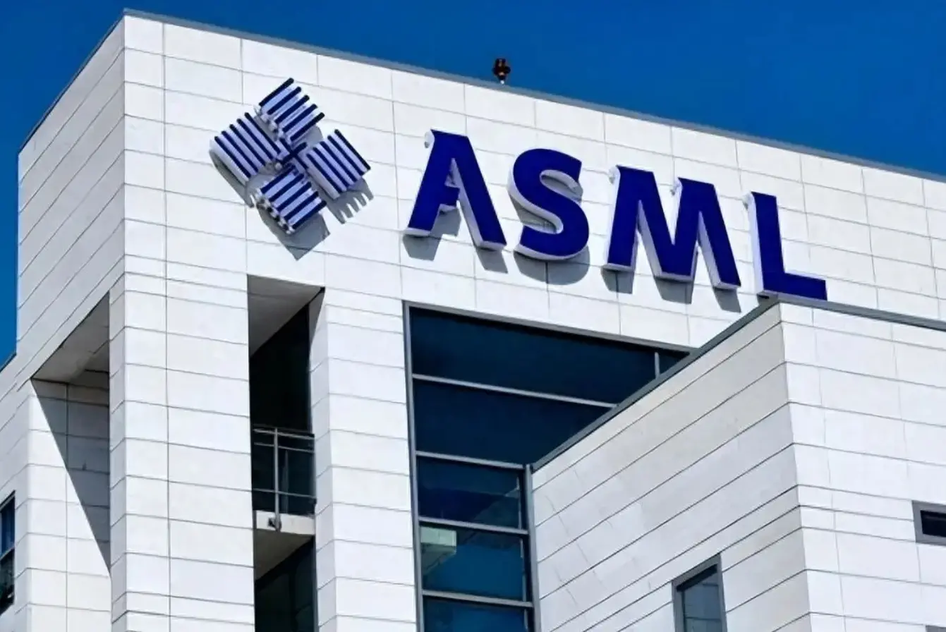
ASML’s second-quarter results came in well ahead of expectations, prompting a swift and broadly positive response from major Wall Street banks. The company reported stronger-than-expected revenue, margins and earnings, then raised its 2026 full-year outlook and, more importantly, laid out a rare capacity roadmap for 2027 and 2028 covering both low-NA EUV and immersion DUV tools. That disclosure directly addressed a key market concern: whether AI-driven semiconductor demand can hold up long enough to justify a more aggressive equipment cycle. Goldman Sachs, JPMorgan and Barclays all maintained or reiterated positive ratings after the release, while several analysts argued the update strengthens the case that supply bottlenecks tied to AI infrastructure remain real. The discussion also extended beyond logic chips into memory, where ASML said tight DDR and HBM supply is pushing customers to invest faster. Goldman’s trading desk said that view challenges the bearish narrative that memory pricing will peak by 2028 or that supply tightness will ease materially before then. Investors reacted quickly. ASML shares in Amsterdam rose about 4%, Nasdaq 100 futures added roughly 40 basis points, and SK Hynix’s Seoul-listed shares jumped 8.8%.

500
ASML lifts guidance and maps out 2027-2028 capacity expansion as Wall Street turns broadly bullish