SCA

Ethena
2026-09-11 12:03:06

Ethena launches USDe and sUSDe on TRON, extending digital dollar access

TRON DAO and Ethena Labs said USDe and sUSDe are now live on the TRON network, bringing Ethena’s digital dollar products to one of the largest stablecoin settlement ecosystems in crypto. Users can already bridge both assets to TRON through Stargate Finance, then hold or transfer them on the network. Support in TRON-native DeFi applications, including JustLend DAO and SUN.io, is expected to arrive over the coming weeks, with additional wallet, exchange, and payments integrations planned afterward. The companies said the rollout gives TRON users access to an extra dollar-denominated asset through USDe and to a rewards-bearing digital dollar product through sUSDe. Ethena, in turn, gains access to TRON’s large global user base. According to the announcement, TRON has more than 403 million total user accounts. Justin Sun said the addition expands options for people already using TRON for payments, savings, and value transfer. Ethena founder Guy Young said the move lets users hold a rewards-accruing dollar on a network they already use at scale. The announcement also described the move as the latest step in USDe’s multichain expansion. Ethena said USDe is now supported across more than a dozen networks and integrated with leading centralized exchanges and DeFi applications.


40
Ethena launches USDe and sUSDe on TRON, extending digital dollar access
ASML
2026-09-09 03:18:36

ASML breaks ground on Eindhoven campus with capacity for 20,000 jobs

ASML has started construction on its new BIC North campus in Eindhoven, the Netherlands, with the company saying the site can eventually support as many as 20,000 jobs. According to ASML’s official announcement, the campus covers about 350,000 square meters, and its first phase is scheduled for completion in 2029. That initial buildout is expected to house at least 3,000 employees, with teams mainly relocating from the company’s existing sites. The project, formally named Brainport Industries Campus North, will combine production, logistics and office functions. The groundbreaking ceremony was held on Sept. 8, with Dutch Prime Minister Rob Jetten in attendance. ASML said the new campus will operate alongside its current facilities, including the De Run 1000 headquarters in Veldhoven and the De Run 6000/7000 industrial campus. A central feature of the expansion is ASML’s so-called Flow Factory model for TWINSCAN systems production. The company said the setup links materials and workflows to help module manufacturing scale faster and more efficiently while keeping quality standards in place. ASML added that the design draws on assembly methods used in the automotive and aerospace sectors. The company did not disclose the investment amount for the expansion.

100
ASML breaks ground on Eindhoven campus with capacity for 20,000 jobs
Samsung Elect
2026-09-08 08:34:52

Samsung targets 2028 DRAM production with High-NA EUV as mask format shifts to 12 inches

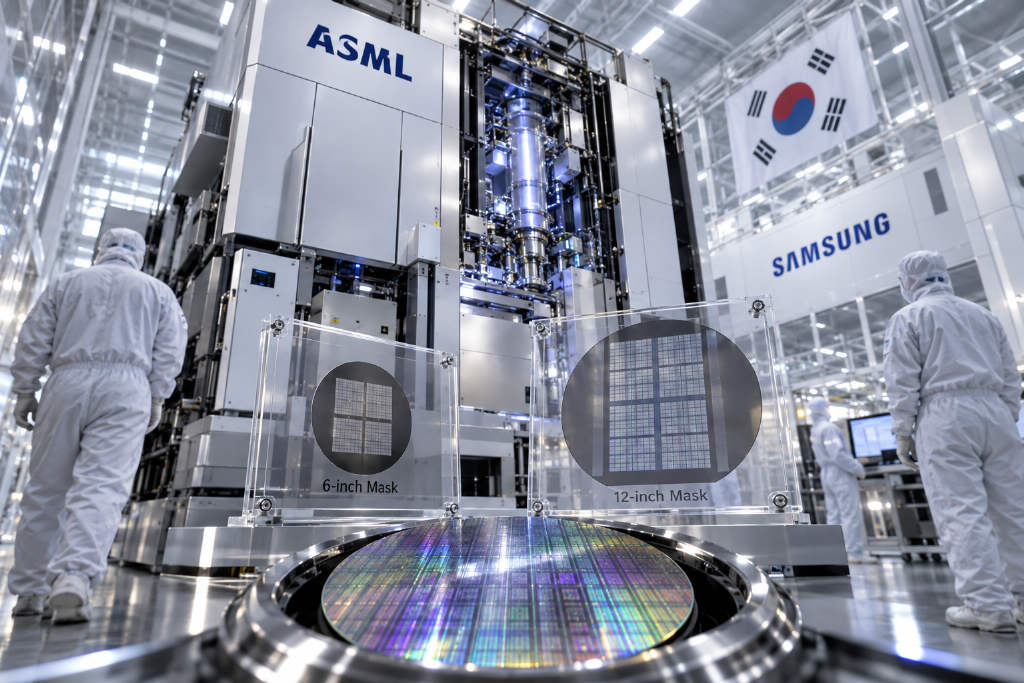
ASML released separate High-NA EUV updates with Intel and Samsung in the same week, outlining progress in both logic and memory manufacturing. Intel Foundry and ASML said at the SPIE Mask Technology and Extreme Ultraviolet Lithography conference that High-NA EUV has processed more than 1 million wafers in total. That figure covers tool verification and testing, research and development, and volume production of selected layers for Intel Core Ultra Series 3 processors, codenamed Panther Lake. The companies said the number does not mean 1 million commercial Panther Lake wafers, and they did not break down how much came from testing, R&D, or production. Samsung, meanwhile, said it plans to introduce High-NA EUV into future DRAM mass production in 2028, marking the first time a memory maker has given a timetable for using the technology in manufacturing. Intel also said it has spent three years advancing a larger mask initiative with ASML and industry partners, while Samsung said it is joining the push for next-generation 12-inch mask technology. The announcements point to a broader infrastructure shift, with mask standards moving from the long-used 6-inch format toward 12 inches.

200
Samsung targets 2028 DRAM production with High-NA EUV as mask format shifts to 12 inches
CatFee.IO
2026-09-01 03:29:18

CatFee.IO Staking Vault Surpasses 620M TRX, Ranks 7th on TRONSCAN DeFi TVL

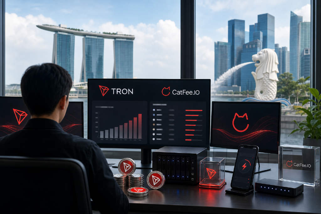
CatFee.IO's Staking Vault has accumulated over 620 million TRX in total staked assets, while cumulative rewards distributed to participants have surpassed 40 million TRX, according to project data. On TRONSCAN's DeFi TVL ranking, the vault currently holds the No. 7 position on the TRON network and is classified under the Staking | Yield category. CatFee.IO has been building TRON-focused resource infrastructure for some time, with a service lineup that spans TRON energy, Staking Vault, node services, enterprise-grade APIs, and Seamless Energy. Seamless Energy is aimed at wallets, exchanges, and enterprise applications, automating energy preparation during transaction broadcasting via nodes and APIs. The approach removes the need for users to manually buy and manage energy ahead of each transaction. With staking volumes continuing to grow and infrastructure products such as Seamless Energy rolling out, CatFee.IO is broadening the application scenarios of its resource services on the TRON chain. The latest figures reflect continued momentum for the project's staking and infrastructure offering.

190
CatFee.IO Staking Vault Surpasses 620M TRX, Ranks 7th on TRONSCAN DeFi TVL
memory
2026-08-09 08:56:07

'New Stock God' Remains Bullish on Memory, Says Photonics Fundamentals Intact

According to ChainCatcher, a figure dubbed the 'New Stock God' has reiterated their bullish stance on memory chip makers, including Micron (MU) and Samsung, arguing that markets tend to rotate between different supply bottlenecks. This week, photonics names from AXTI to LITE are back in focus; compared with the July selloff, the main change has been in share prices, followed by scattered narratives and business updates. The investor noted that the market already knew during July that COHR and LITE's laser products were sold out for the next two years and had learned about demand imbalances from AAOI's last quarter's earnings call. Aside from post-liquidation price moves, photonics fundamentals have not deteriorated; bottlenecks in optical transceivers and indium phosphide substrates remain unchanged, possibly even worsening. On memory, the 'New Stock God' said retail investors are showing capitulation, though the same crowd was extremely bullish after MU signed 16 SCAs and delivered solid guidance. They believe the current ratio of memory operating profit to market cap is 'extremely unreasonable,' and demand imbalance may worsen next year. The same companies have only seen changes in valuation and narrative, while the market rotates across sectors.

1100
'New Stock God' Remains Bullish on Memory, Says Photonics Fundamentals Intact
Coldcard
2026-08-05 11:34:27

Coldcard RNG flaw tied to four suspected attack waves as scrutiny grows over Bitcoin self-custody risks

A years-old randomness flaw in Coldcard hardware wallet firmware has come under intense scrutiny after several waves of suspicious Bitcoin sweeps were linked by researchers to seeds created under affected software versions. Investigations by Block and Coinkite traced the issue to a 2021 code migration that routed seed generation through a software pseudorandom number generator instead of the intended hardware RNG on some firmware paths, reducing the effective search space of wallet seeds below the design target. Galaxy Research said three suspected attack waves it identified covered 4,585 addresses and 1,367.05 BTC, and on Aug. 3 its researchers flagged a fourth wave that was later updated to about 448.7 BTC across 709 potential victim addresses. Those figures come from on-chain pattern analysis and are not a wallet-by-wallet confirmation of Coldcard victims or final losses. The incident has also reopened debate over custody models. Researchers and market observers pointed to higher address activity, movements from older UTXOs, and inflows to centralized venues after the disclosure, while cautioning that on-chain data alone cannot prove those moves were caused by the Coldcard bug. Coinkite has said users with affected seeds need to generate a new seed in patched firmware or another trusted environment and move funds, because updating firmware alone does not restore the missing entropy in an already created mnemonic.

1390
Coldcard RNG flaw tied to four suspected attack waves as scrutiny grows over Bitcoin self-custody risks
Huawei
2026-08-05 06:36:19

Huawei scientist says Nvidia-led chip path is nearing physical limits, first Tau-based phone chip due later this year

Huawei chief semiconductor scientist Liao Heng said in a recent public livestream that the conventional path pursued by major Western chipmakers, including Nvidia, is approaching hard physical manufacturing limits. According to Bloomberg, Liao argued that the long-running strategy of shrinking transistors is running into diminishing returns even as companies build larger chips, pack in billions of transistors and add more high-bandwidth memory. She said Huawei, cut off from key lithography tools under U.S. sanctions, has been forced onto an alternative path. That route is built around the company’s self-developed Tau Scaling Law, formally introduced in May at the IEEE International Symposium on Circuits and Systems. Instead of geometric scaling, the framework focuses on “time scaling” by reducing signal propagation time and speeding data transfer across system components. Huawei says it has designed and mass-produced 381 chips under this approach over the past six years. Liao also said Huawei’s first smartphone chip built on the framework, using its LogicFolding technology, will be released later this year. She described the launch as a key real-world test of the company’s alternative roadmap. In the same livestream, Liao pointed to DeepSeek as proof that better design can offset limited compute resources and said the global semiconductor supply chain is moving toward two separate ecosystems as U.S.-China tensions deepen.

1080
Huawei scientist says Nvidia-led chip path is nearing physical limits, first Tau-based phone chip due later this year
Kioxia
2026-08-05 00:09:52

Kioxia and Sandisk unveil 332-layer QLC 3D NAND with 4,800 MT/s interface

Kioxia and Sandisk introduced their latest BiCS10 3D QLC NAND flash chip at the Future of Memory and Storage Conference on Aug. 5, describing it as the highest-density 3D NAND product that has been formally launched worldwide. The chip uses a 332-layer stack and reaches a storage density of 37 Gb/mm², with interface speeds of up to 4,800 MT/s and support for Separate Command Address, or SCA. The companies said the product is aimed at high-capacity data center SSDs. Compared with their earlier BiCS10 3D TLC NAND, which delivered storage density above 29 Gb/mm², the new QLC version pushes capacity density higher for data center storage. Industry estimates cited in the report said the chip could reach roughly 1.33 Tb under similar die size and memory cell count assumptions, though the companies have not disclosed an official capacity specification. Kioxia and Sandisk also introduced PI-LTT technology to improve high-speed signal integrity while reducing output driver power consumption. The two companies said the latest BiCS10 process could also help lower manufacturing costs after production ramps up.

1360
Kioxia and Sandisk unveil 332-layer QLC 3D NAND with 4,800 MT/s interface