
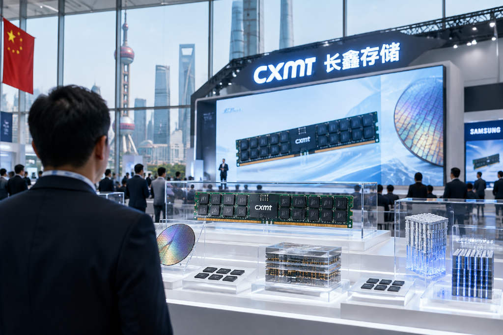
ChangXin Memory Technologies (CXMT) has laid out a new DRAM technology timeline, with company president Dr. Cao Kanyu saying in Shanghai that CXMT expects to launch a next-generation DDR5 RDIMM server memory product by the end of the year. The product is set to combine a 4F² memory cell architecture with hybrid bonding and other technologies.
CXMT’s first 4F² DDR5 RDIMM is aimed at the server segment
According to the report, Cao used his speech at the fourth Integrated Chip and Chiplet Conference to detail CXMT’s work in DRAM devices, 4F² architecture, and hybrid bonding. He also said the company plans to bring those technologies together in a new DDR5 RDIMM product by year-end.
RDIMM, short for Registered DIMM, is a mainstream memory module format in the server market. It uses a register to buffer command and address signals from the processor, reducing electrical load and allowing a single motherboard to support more high-capacity modules. In the report’s reading, CXMT’s decision to make DDR5 RDIMM the first product for its 4F² architecture shows a clear focus on server memory.
What 4F² changes in DRAM design
Mainstream DRAM today uses a 6F² memory cell, where each cell consists of one transistor and one capacitor. In a 4F² design, the transistor and capacitor are stacked vertically, cutting the cell area to four times the square of the minimum feature size, or F.
Under the same line width, that can reduce cell area by about 33%, with theoretical density gains of roughly 30% to 50%. The shift from 6F² to 4F² is not a simple process shrink, though. The report said existing manufacturing flows cannot be reused directly and that a new device and process system has to be built.
Cao said CXMT has optimized several key steps, including word-line metallization, bit-line formation, and junction activation. On the R&D side, the company has disclosed more than 300 patent families related to 4F² and published mainland China’s first paper on a 4F² architecture in 2021.
Wccftech says the timing could put CXMT ahead of Samsung
Wccftech, citing Samsung’s 4F² roadmap, said Samsung is planning to introduce the architecture in 2028. Citrini researcher Zephyr also said Samsung may separate the memory cell and peripheral circuitry into different manufacturing flows and then stack them through wafer-to-wafer hybrid bonding.
If CXMT launches on schedule by the end of this year, its introduction timing would come about two years before Samsung’s. The report also said Samsung’s future products could carry higher pricing because hybrid bonding is expensive.
Wccftech added an important caveat: CXMT’s first-generation product is more likely to be a partial derivative based on a 15 nm-class G5 process rather than a full 4F² implementation. In that sense, being “ahead” refers to introduction timing, not necessarily overall product competitiveness or mass-production scale.
Capacity, HKMG, and customer validation remain key questions
Wccftech also said CXMT’s monthly capacity is expected to reach about 300,000 wafers by year-end across three DRAM fabs, with another roughly 50,000 wafers of HBM capacity. After new plants in Shanghai and Hefei are completed, monthly capacity could rise to 600,000 wafers, and the company may surpass Micron in production scale by 2030.
On process technology, the report said CXMT is applying high-k metal gate, or HKMG, to its G4 DRAM process and LPDDR5X products to reduce leakage, improve power efficiency, and raise speed.
Market analyst Fred Chen said CXMT has already mass-produced G5 and uses self-aligned quadruple patterning, or SAQP, as one of its key process technologies. Attention is now on the specifications CXMT will disclose at year-end, the actual yield and production schedule of its 4F² products, and the pace of validation and adoption by server customers.