
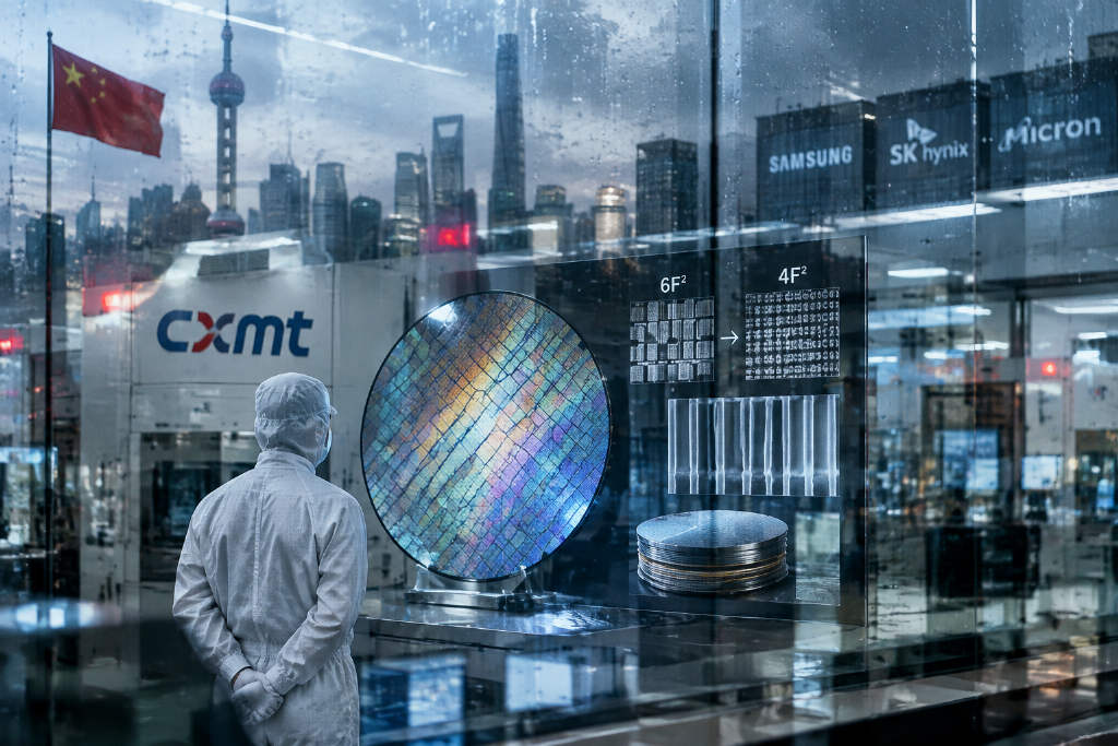
Changxin Memory Technologies said it has made major advances in DRAM devices, 4F² architecture and hybrid bonding, a development that the source article says pushed shares of the three overseas memory makers lower as investors reassessed the pace of China’s catch-up in DRAM.
The market concern described in the report centers on two points. If a Chinese manufacturer breaks through a key technical barrier, production scaling can move quickly. At the same time, 4F² is itself a structure that directly improves output per unit area. Taken together, that could mean China’s effective DRAM supply grows faster than previously expected.
The two changes drawing the most attention are the shift from the mainstream 6F² cell layout to 4F² and the self-developed VSG transistor, short for Vertical Surrounded Gate, that makes that layout possible. Their immediate importance lies in density: at the same node, a 4F² cell is about one-third smaller than a 6F² cell, which is equivalent to fitting about 50% more memory cells into the same area and lifting DRAM bit output materially.
To frame the impact on the memory industry and on Samsung Electronics, SK hynix and Micron, the source article first breaks down the underlying technology. It asks four questions: how DRAM cells and arrays are built, what really changes from horizontal transistors and 6F² to vertical surround-gate transistors and 4F², why 4F² is difficult and whether it is unique to CXMT, and how much all of this could matter for the industry.
The DRAM cell starts with a 1T1C structure
One transistor, one capacitor
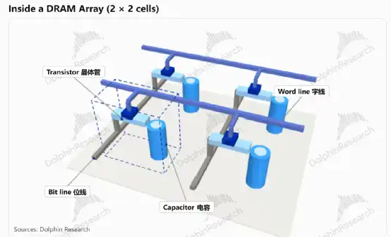
The basic DRAM storage unit is a cell. In a 1T1C design, one transistor and one capacitor form the smallest storage element, and that element stores 1 bit.
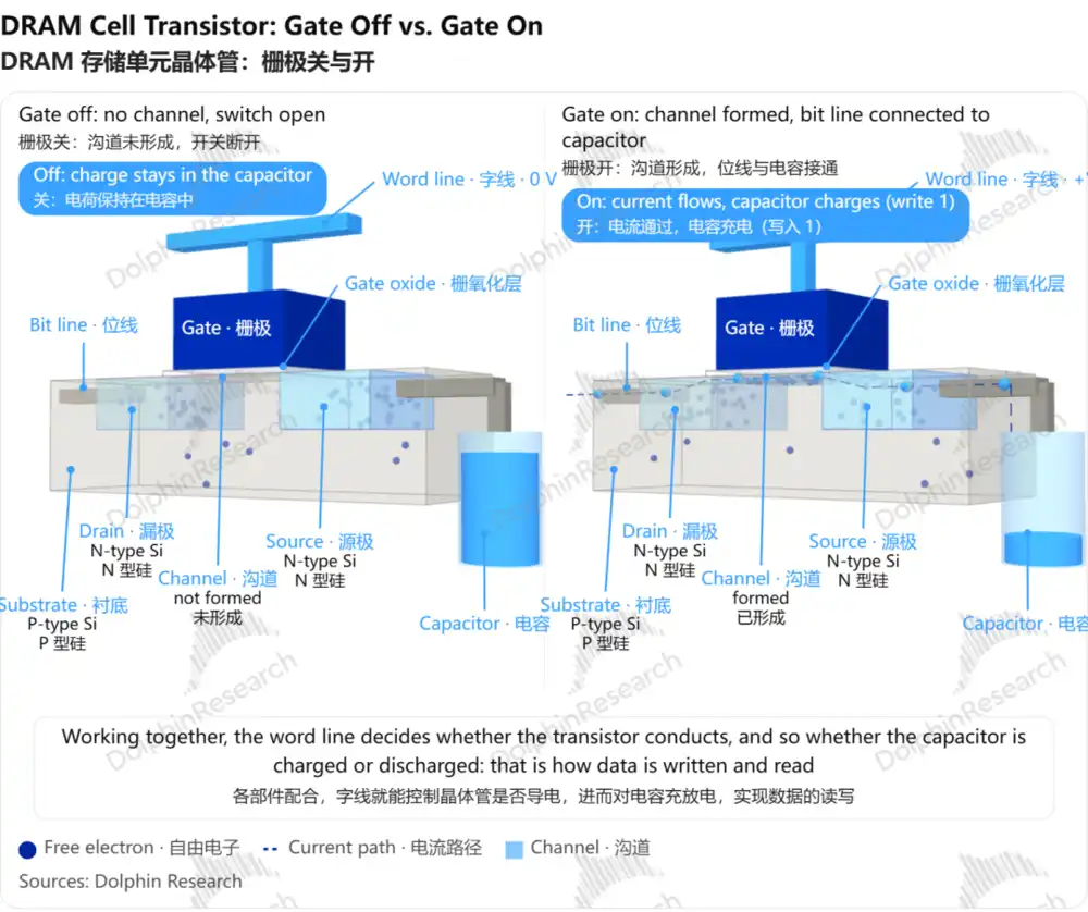
The capacitor is where data is actually held. Stored charge represents binary data: charge means 1, no charge means 0. The transistor acts as a switch, controlling whether current can flow between the capacitor and the bit line. When the switch is on, data can be written or read. When it is off, charge remains in the capacitor.
The transistor itself contains several key parts. The source and drain are two terminals, with one connected to the capacitor and the other to the bit line. Both are N-doped silicon and contain many freely moving electrons, so they conduct. Between them is a P-type silicon substrate, which has relatively few mobile electrons and therefore does not conduct in its default state. Above that region sits the gate, separated from the silicon by a gate oxide layer only a few nanometers thick. The gate connects to the word line. When a positive voltage is applied to the gate, the electric field pulls electrons in the substrate toward the silicon surface under the oxide, creating a conductive channel and connecting source to drain. Remove the voltage and the channel disappears.
That is how a word line controls a gate, the gate controls a channel, and the channel determines whether the capacitor can be charged or discharged.
Word lines and bit lines turn cells into arrays
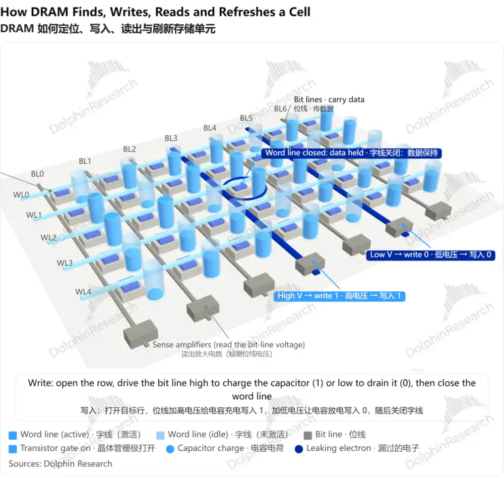
A single cell stores only 1 bit, but a DRAM chip contains tens of billions of them. They have to be packed tightly and still be individually addressable, so DRAM uses a matrix with crossed rows and columns. Horizontal word lines choose a row. Vertical bit lines carry data.
A word line connects the gates of every transistor in the same row. Apply voltage to one word line and all transistors in that row turn on together, while other rows remain off. A bit line connects the drains of all transistors in the same column and then to their capacitors, allowing data to be written and read. Because each cell sits at the intersection of one word line and one bit line, memory addresses are split into row and column addresses that together identify a single cell.
Writing works like this: activate the target word line and open the transistor; apply high voltage on the bit line to charge the capacitor and write 1; apply low voltage to discharge it and write 0; then close the word line. Reading opens the transistor and lets any stored charge flow to the bit line, producing a tiny voltage change that determines whether the bit is 0 or 1. Refresh is necessary because reading itself consumes charge and because slight leakage is unavoidable even when the transistor is off. Charge gradually drains away, so each cell must be periodically read and written back. That is why DRAM is called dynamic memory.
The article highlights two leakage sources. The first is that the P-type substrate is not perfectly insulating even when the gate is off, so a small number of electrons can still leak through. The second is that leakage becomes easier as capacitors shrink. A shorter substrate raises the chance of leakage and data loss, one of the reasons density and process precision cannot be increased indefinitely without side effects.
From 6F² to 4F²: what changes physically
The mainstream 6F² layout keeps the transistor horizontal
The topology above describes electrical connections. What determines area and bit output is the physical layout on silicon.
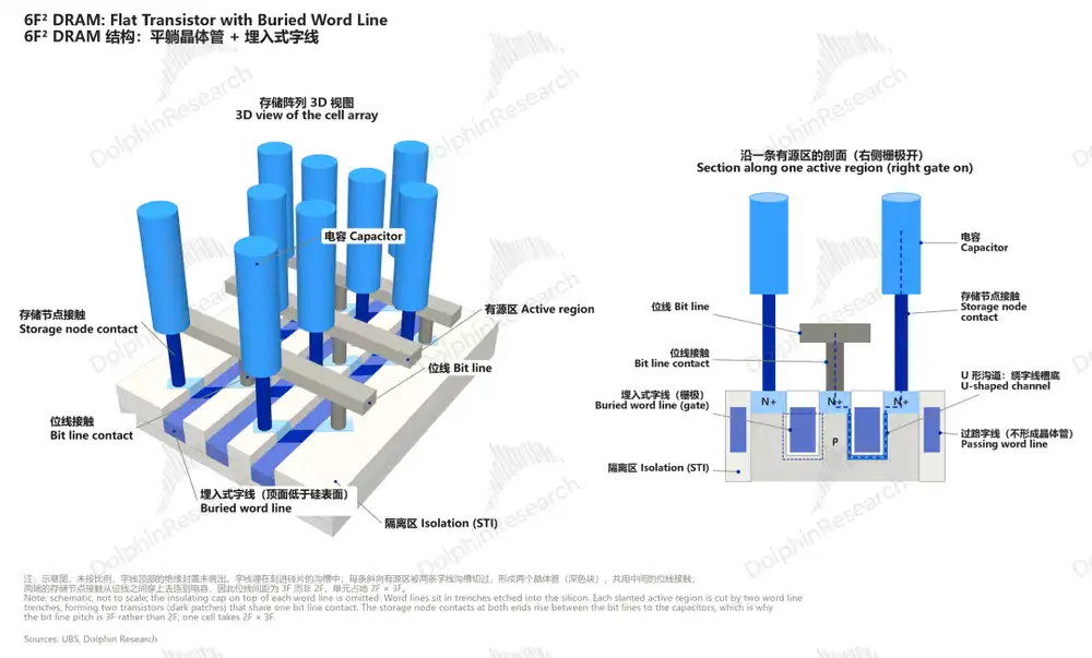
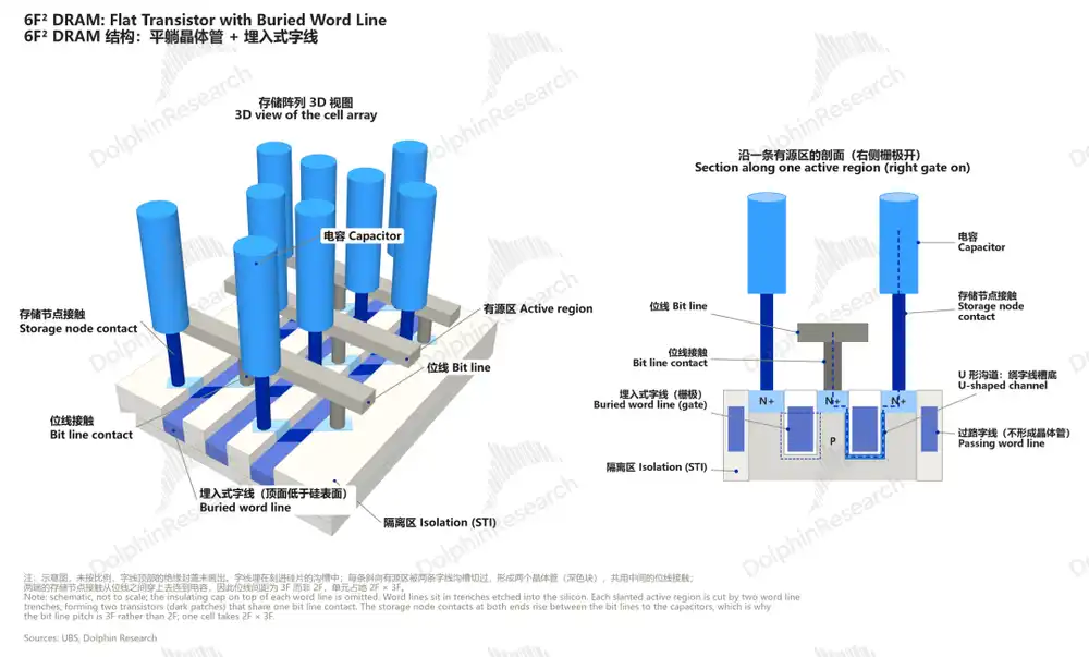
Mainstream DRAM today uses a 6F² layout. From bottom to top, it roughly consists of a transistor and word-line layer, then a bit-line layer, then the capacitor layer on top.
In this structure, transistors lie horizontally on the silicon surface, often in pairs. Diagonal strips of single-crystal silicon, called active regions, are arranged across the wafer surface and separated by insulating isolation regions. Each strip is crossed by two word lines, creating two controllable transistor switches. Portions not crossed by word lines act only as conductors. As a result, one active strip serves two capacitors while sharing one bit line.
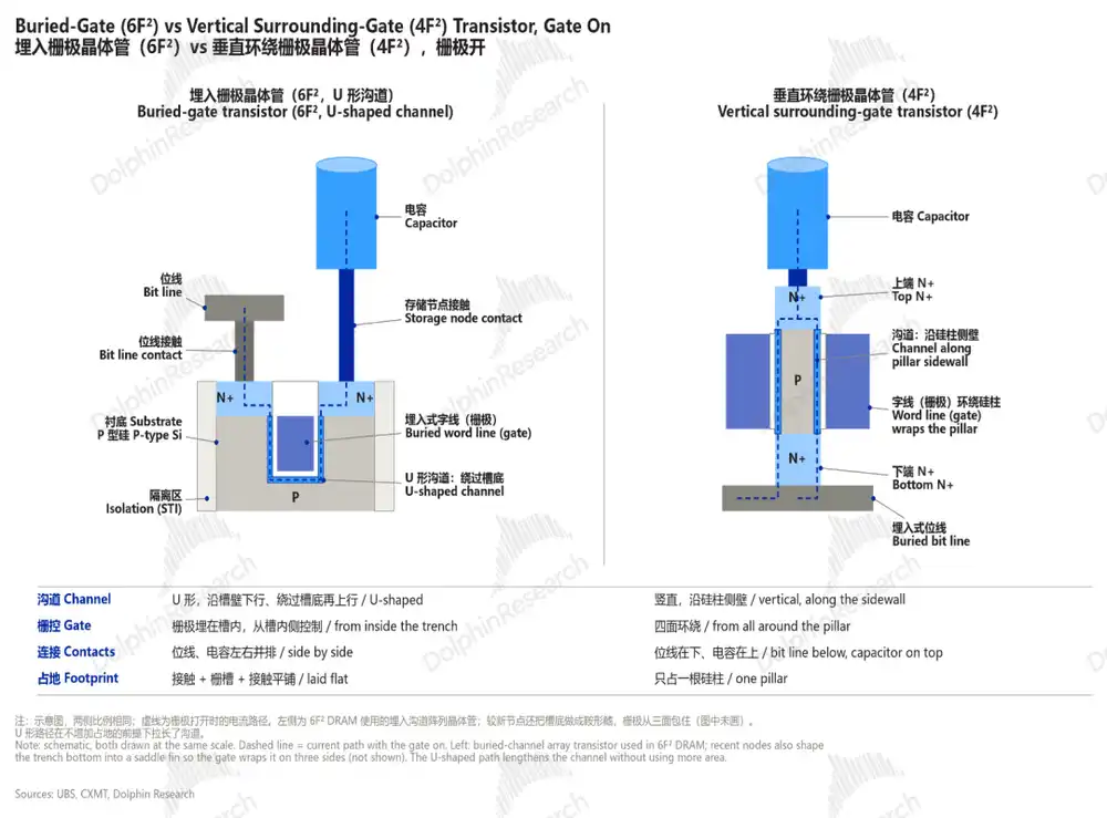
To suppress leakage caused by short-channel effects, 6F² no longer uses a textbook planar transistor. Instead, trenches are etched into the single-crystal silicon strip and the word line, meaning the gate, is buried inside the trench. That extends the channel without increasing footprint. Even so, the transistor remains a horizontal device.
Here, F stands for feature size, the minimum line width a process can form on a chip. Each new DRAM generation, such as 1a, 1b or 1c, is essentially a smaller F. The industry uses multiples of F² to describe cell area. A 6F² cell occupies six squares with side length F, while 4F² occupies four, which makes area efficiency comparable across architectures.
VSG turns the transistor upright and wraps the gate around it
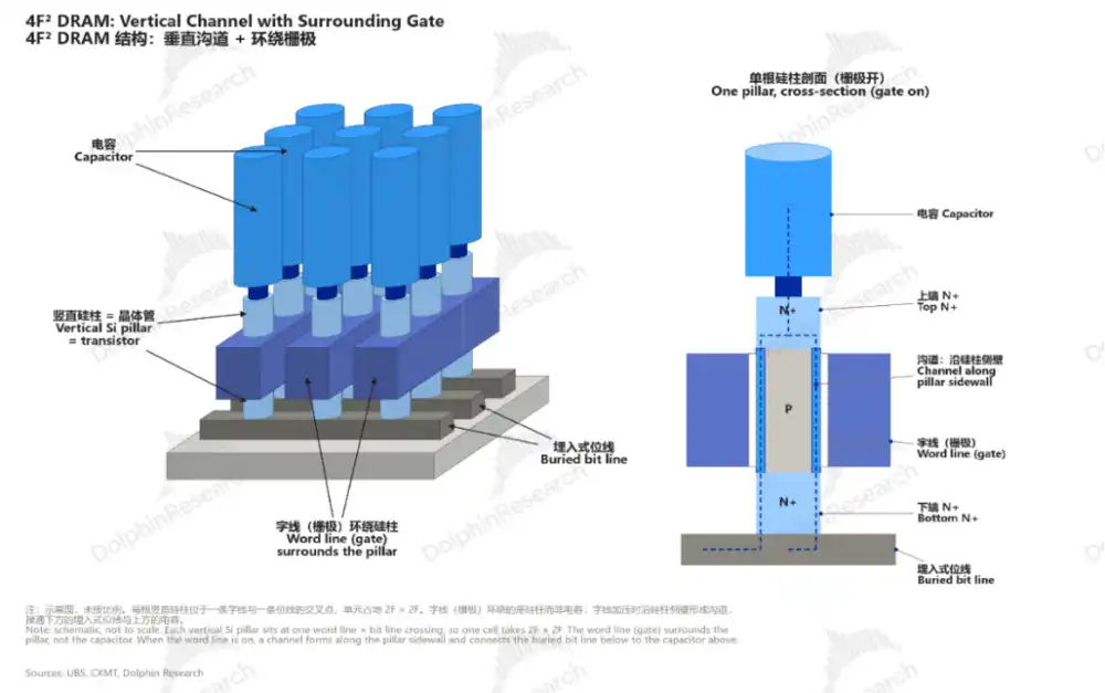
The starting point for 4F² is a new transistor shape. Instead of a horizontal strip, the transistor becomes a vertical column. That is why it is called VSG, or Vertical Surrounded Gate.
Compared with a conventional transistor switch, VSG changes two things. First, the transistor stands vertically instead of lying flat. Second, the gate no longer sits only above one side of the channel. It surrounds the entire channel.
That structural shift has several direct effects.
One, channel length is no longer tied to footprint. In a horizontal device, source, channel and drain spread laterally, so a longer channel takes up more horizontal area. In a vertical device, channel length is set by the height of the silicon pillar and is decoupled from the horizontal footprint. That means higher cell density no longer has to come at the cost of a shorter channel, easing one of the bottlenecks created by short-channel leakage.
Two, gate control is stronger. In a horizontal structure, the gate mainly controls the channel from one side. In a vertical silicon pillar, the gate surrounds the channel, so the electric field acts from all sides and shuts the channel off more completely. For DRAM, lower leakage means longer charge retention, potentially lower refresh frequency, lower power and more time available for normal read and write operations.
Three, the capacitor, bit line and word line can be stacked vertically, so the capacitor no longer has to snake through the gaps between bit lines. In 6F², the flat transistor has one contact going to the bit line and another going upward through the bit-line layer to the capacitor above. That forces the capacitor contact to pass between neighboring bit lines and maintain insulation spacing from both sides, so the bit lines cannot be packed as tightly as possible. In 4F², the bit line sits below the silicon pillar, the word line wraps around its middle and the capacitor sits above it. The capacitor contact no longer needs to pass through a lateral gap between bit lines, which is the direct reason the cell can shrink.
Why 4F² can reduce area so sharply
DRAM scaling aims to fit more cells into a given area while preserving charge retention and read reliability. That scaling runs into two limits: transistor leakage and capacitor capacity. As the capacitor footprint shrinks, maintaining enough stored charge requires making the capacitor taller, increasing aspect ratio and making etch and deposition harder, with more yield risk.
4F² sidesteps that problem at the architectural level. It shrinks the cell without first shrinking F. In a 6F² design, the capacitor contact must pass between adjacent bit lines, so bit-line pitch is forced to 3F while word-line pitch is 2F. The cell area is therefore 2F by 3F, or 6F². In 4F², the capacitor sits directly above the pillar, so the bit lines no longer need extra spacing for the capacitor contact. Bit-line pitch can drop to the minimum 2F, making the cell area 2F by 2F, or 4F².
At the same process node, that cuts cell area by about one-third. The array-level result, in theory, is up to a 50% gain in storage density because the same area can hold 1.5 times as many cells.
But a DRAM die is not only an array. It also contains peripheral circuitry such as sense amplifiers, decoders and word-line drivers. Those areas do not automatically shrink when the cell architecture changes. As cells become denser, fitting the peripheral blocks around the array can actually get harder. That is why chip-level density gains fall short of the full 50%. The report says media references to a 30% to 50% increase in single-chip storage density broadly reflect that discount.
That also explains why the industry has leaned toward placing peripheral circuitry on a separate wafer and then stacking it under the DRAM array through hybrid bonding. Only then can more of the array-level density gain show up at the chip level. CXMT’s emphasis on decoupling DRAM and CMOS processes plus wafer-level hybrid bonding fits this logic.
The article cites UBS as estimating that first-generation 4F² relaxes process precision by about 30%, equivalent to saving roughly two generations of node shrink. UBS also estimates that the capacitor wall dimensions at the first 4F² node are roughly comparable to those at the 1c node. For CXMT, which is subject to export controls and cannot use EUV, that point is especially important. Continued 6F² scaling depends more and more on EUV or on more complex multiple patterning, while 4F² can deliver a density gain without requiring narrower lines at the outset.
The report adds one caution. The gain from moving from 6F² to 4F² is a one-time architectural benefit. After first-generation 4F², every company still has to continue shrinking F. According to an April report from The Elec cited in the article, Samsung plans to use 4F² through its 10a, 10b and 10c generations before moving to 3D DRAM. A September Korean media report cited by the article says Samsung and SK hynix both plan to introduce High-NA EUV into DRAM mass production around 2028.
4F² is not unique to CXMT, and each major supplier has a timeline
Samsung, SK hynix, Micron and CXMT are not moving at the same speed
The source is explicit that 4F² is not a CXMT-only invention. Research on vertical-channel transistors has existed for years. One reason it was previously set aside is that the memory array and peripheral logic were tied to one process flow, making a 6F² architecture change less attractive from a cost-benefit perspective. As further 6F² scaling became harder and integration methods like hybrid bonding matured, 4F² returned as a widely recognized next-generation path.
Based on the industry checks cited in the article, all three global memory leaders are evaluating 4F², and some have already moved their adoption plans forward.
- Samsung: The report describes Samsung as the fastest so far, though with some shifts in direction. According to The Bell in August, Samsung had planned to complete 1d development in September this year, move into mass production in December and begin initial volume output around the end of 2027, with the next-generation 0a node, which Samsung calls 10a, originally set to transition to 4F². The Elec reported in April that Samsung had already produced wafers on the 10a process in March and confirmed functioning chips in testing, with development to be completed this year, qualification in 2027 and transfer to production lines in 2028. The article says Samsung appears to lead the other two on 4F² R&D and preparation.
- SK hynix: Likely one node later. The Elec reported in April that SK hynix plans to bring in 4F² and vertical transistors at the 0b node, one generation behind Samsung. The Bell said in August that SK hynix planned to complete 1d development in December this year, while Samsung had targeted September. That puts SK hynix about three months behind on development completion and roughly half a year behind on production preparation at 1d, which helps explain the slower migration to 4F².
- Micron: The roadmap remains less clear, and the article treats Micron as the likely laggard. Micron has not publicly detailed its 4F² adoption plan. One Korean media report in 2025 said Micron might skip 4F² and move directly into 3D DRAM research, while UBS said in an industry survey this January that Micron had recently put 4F² back on its roadmap, with 0a moving to 4F² and mass production expected in the second half of 2030.
- CXMT: The company has announced a first-generation product, but not a confirmed mass-production scale. According to recent remarks from the president of CXMT cited in the article, the first-generation 4F² product is aimed at DDR5 RDIMM and is expected to be introduced by year-end. That would be earlier than the currently disclosed mass-production windows of the three major overseas suppliers. Still, the language used was “launch” rather than “mass production,” and there is no disclosed product specification, yield or shipment scale. The year-end milestone could therefore amount to a release, customer sampling or small-batch verification.
Why 4F² is hard: the challenge is manufacturing, not the idea
The article groups the difficulty of 4F² into five main areas.
The first is the floating-body effect. Because the bit line sits at the bottom of the silicon pillar, it separates the pillar from the silicon base below. The P-type silicon in the middle of the pillar becomes effectively floating, allowing charge to accumulate without a natural discharge path. The report compares it to electrical equipment without grounding. That can shift threshold voltage and lead to data loss or errors. One solution under study is the use of a back gate to suppress the effect.
The second is process sequencing. “Build the bit line first, then grow the silicon pillar” is not easy. Since the new structure puts the bit line under the pillar while the pillar itself requires high-quality single-crystal silicon, one route is to grow the pillar epitaxially above the bit line, but epitaxy capacity and uniformity are both difficult. Another route is a backside process: make the silicon pillar from the front side, flip and thin the wafer, then form the bit line at the bottom of the pillar from the backside. That usually requires special wafers such as silicon-on-insulator, adding steps and complexity. A third route is to fabricate the silicon pillar and bit line on separate wafers and then face-bond them through hybrid bonding so the copper contacts connect directly. The article notes that this approach is already used in volume production in 3D NAND, citing YMTC’s Xtacking as an example.
The third difficulty is process decoupling between the memory array and peripheral circuitry. The vertical transistor array and the surrounding logic have very different process requirements, and putting them on the same wafer causes tradeoffs for both. The article says that was one reason early 4F² exploration stalled. CXMT’s disclosed route separates manufacturing and then integrates the two through wafer-level hybrid bonding, which creates fresh demands on bonding yield, alignment accuracy and cost.
The fourth is materials and resistance. In a 4F² structure, only about 1F of space remains between two neighboring rows of silicon pillars. The gate oxide on both sides, the surrounding word lines and the insulating layer between word lines all have to fit inside that gap, leaving very limited room for word-line metal. Bit lines face similar restrictions. As lines get thinner, resistance rises and signal transmission slows, which hurts memory performance. The industry is therefore evaluating molybdenum and ruthenium as alternatives to titanium nitride and tungsten for word lines, because the resistance penalty is smaller at very fine dimensions.
The fifth is interference and yield ramp. Tighter packing of pillars and word lines strengthens coupling between neighboring word lines. On top of that, design and process flows from the 6F² era cannot simply be reused. A first-generation product needs a newly integrated process stack, and it usually takes time to raise yield.
The article’s bottom line is that CXMT’s announcement shows 4F² has moved from a question of whether to pursue the architecture to a question of whether it can be built. But when it can be mass-produced, and how well, is a separate question.
Industry impact: limited near term, but supply could look different after 2028
The source returns to the opening question of how much CXMT’s 4F² progress could affect the memory industry and the three global leaders. Its answer is split into the near term and the medium to long term.
Near term: 2026 to 2027, little direct change to supply and demand
In the short run, the article argues that the direct impact on the supply-demand balance is limited. CXMT has only previewed the product, and it is a first-generation design with specifications, yield and production scale still unknown. New architectures usually take time to ramp from first release to becoming a meaningful share of capacity. In addition, based on the mass-production schedules cited for the three major manufacturers, products built on 4F² are more likely to begin releasing in size toward the end of 2028. For the currently visible supply-demand picture, the market is effectively only seeing out to 2028, so the architecture should not yet alter fundamentals very much.
Under that interpretation, the recent weakness in the three majors’ share prices reflects concern about CXMT’s catch-up speed more than any immediate change in fundamentals.
Medium to long term: after 2028, supply growth may face upside risk
Beyond that window, the calculation changes. The article says 4F² effectively pulls forward about two generations of density improvement in one step, raising bit output by 30% to 50% even if wafer output does not change. It also cites a forecast from the source author that nearly 75% of new DDR wafer capacity added from 2026 to 2028 will already come from domestic Chinese suppliers, and that estimate does not include any extra output enabled by 4F².
If CXMT really can mass-produce 4F² DDR in 2027, the release of supply could be materially higher than earlier expectations. Without enough demand growth, the market could swing sharply and memory prices could fall clearly.
The article adds that although CXMT has not yet broken through in HBM, DDR and HBM currently have almost similar prices per GB, while DDR costs less to manufacture. That makes DDR the main profit contributor for memory companies at present. Based on the author’s earlier estimate, more than 70% of SK hynix’s DRAM gross profit in 2028 would come from conventional DDR. If CXMT’s new 4F² products can ramp both capacity and yield smoothly, the effect on the profit pools of the three major memory makers could be substantial.
The implications differ by company
CXMT: an alternative catch-up route that does not rely on EUV
For CXMT, the biggest significance is that 4F² offers a route to narrow the technology gap without EUV. As 6F² scaling advances, dependence on EUV becomes greater. CXMT cannot access EUV because of export controls and must rely on DUV multiple patterning, which raises cost and yield pressure generation after generation. By trading architecture for density and relaxing design rules, 4F² gives CXMT a chance to approach the storage density of its global rivals under DUV conditions.
The report also points to CXMT’s ongoing capacity expansion and the fact that its first product is aimed directly at server DDR5, a higher-barrier and higher-profit part of the conventional DRAM market. That could increase competitive pressure in commodity DRAM.
Samsung: a chance to convert technical lead into a comeback
The article says Samsung’s yield issues in recent DRAM generations have also weighed on its HBM progress. But Samsung appears relatively advanced both in process development and in 4F² preparation. That could open a chance for it to recover ground and move from lagging to leading in newer products.
SK hynix: little immediate effect, but Samsung’s execution bears watching
For SK hynix, the source sees limited short-term impact. SK hynix is one node behind Samsung on 4F² timing, but its current strength is mainly built on HBM products and customers, and 4F² timing alone does not quickly change that. The bigger issue is whether Samsung can use 4F² to repair execution in DRAM and HBM, because that could narrow SK hynix’s lead in HBM.
Micron: relatively exposed if others move first
Micron has been more focused on the 3D DRAM route. If UBS’s estimate is correct and Micron’s 4F² mass production does not arrive until the second half of 2030, Micron could face a period of relative disadvantage in cost and density if Samsung and CXMT get there first.
Upstream suppliers: new process steps may create equipment and materials demand
For the upstream chain, 4F² adds many process steps, including selective epitaxy, atomic layer deposition, rapid thermal processing, high-aspect-ratio etch and hybrid bonding. The article identifies Applied Materials, Tokyo Electron, Lam Research, ASMI and Eugene Tech among potential beneficiaries on the equipment side, and suppliers of new materials such as molybdenum and ruthenium, with Merck cited on the materials side.
At the same time, the report says first-generation 4F² could dilute lithography demand to some extent, though later node upgrades will still depend on smaller geometries and more advanced lithography tools.
The article originated from the WeChat public account Dolphin Research and was written by an author identified as Dolphin Jun. Its original Chinese headline was “CXMT turns the transistor vertical: can a catch-up path that bypasses EUV shake the three memory giants?”