
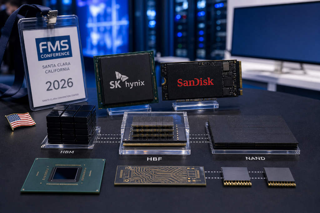
SK hynix and SanDisk put HBF on the map at FMS 2026
SK hynix and SanDisk unveiled the first HBF (High Bandwidth Flash) specification and roadmap at the 2026 FMS Conference in Santa Clara, California. The first release targets up to 512GB of capacity, with bandwidth across grades ranging from about 0.4 TB/s to 3.0 TB/s. HBF will use UCIe (Universal Chiplet Interconnect Express) as the link between the memory device and the processor.
SanDisk also presented a test case showing that, in a specific AI inference scenario, four GPUs paired with 4TB of HBF produced nearly the same number of tokens per second as eight GPUs paired with 192GB of HBM. In that setup, GPU usage efficiency was about 2x higher, while total cost was lower. The example was reported by Forbes.
Why HBF exists
HBM remains one of the most important memories for AI GPUs. It stacks multiple DRAM layers vertically to deliver very high bandwidth, and it has become a core component in accelerators from NVIDIA and AMD.
But AI workloads are moving beyond training and into large-scale inference. Model weights, RAG data, KV cache, agent state, and metadata are all growing fast. In many cases, relying only on expensive HBM with limited capacity is no longer the most cost-effective answer.
HBF tries to bring the same stacked-memory idea to NAND flash. SanDisk CTO Alper Ilkbahar said HBF packages NAND chips in a way similar to how HBM stacks and connects DRAM, aiming to create a high-capacity, high-bandwidth non-volatile storage layer. It is not necessarily meant to replace HBM. Depending on the workload, it can work alongside HBM, and in some cases it can be used on its own.
SK hynix redraws the AI memory stack
SK hynix used the same conference to present a revised AI memory and storage hierarchy. In addition to HBM at its current G1 level, the company added three intermediate tiers: G0.5, G1.5 and G2.5. The aim is to give different AI workloads a more granular trade-off between performance, capacity and cost.
G0.5 uses 3D-stacked DRAM and sits above HBM, with a goal of offering DRAM-like capacity and SRAM-like bandwidth. G1.5 is HBF, which SK hynix is planning at roughly 1TB of capacity and Tb/s-class bandwidth. G2.5 is shared memory built through CXL pooling, with capacity that can scale into multiple terabytes.
SK hynix said the architecture is designed to maximize xPU performance and QoS, while improving TPS/MW and Token/$.
Inference workloads are pushing KV cache to the forefront
SK hynix EVP Kim Chunsung said AI inference data can be grouped into two broad categories. The first includes persistent assets such as model data, RAG data and user data. The second covers dynamic state created during inference, including KV cache, AI agent state and metadata.
As context windows grow longer, agent sessions last longer, and companies deploy more inference services, storing large amounts of KV cache is becoming a new hardware bottleneck. SanDisk has therefore positioned persistent KV cache as one of the key use cases for a new memory tier, with the goal of shifting some data out of costly HBM and into larger, lower-cost HBF.
Spec details, roadmap and NAND scaling
The HBF Consortium said the first HBF specification supports 8-high and 16-high NAND die stacks and capacity of up to 512GB. Bandwidth is split into Grade 1 through Grade 3, ranging from about 0.4 TB/s to 3.0 TB/s.
Another key design choice is UCIe as the processor interface. UCIe has become a major chiplet interconnect standard in the semiconductor industry. If HBF develops into a full ecosystem, CPUs, GPUs and AI accelerators could integrate high-bandwidth flash through a standardized interface rather than relying on proprietary designs.
SanDisk is also advancing BiCS10 to support HBF. The company showed 218-layer BiCS8 enterprise SSDs, including a Compute eSSD using TLC NAND with up to 32TB of capacity and a Storage eSSD using QLC NAND with up to 256TB. BiCS10 moves further to 332 layers, with TLC NAND at 1Tb per die and QLC NAND at 2Tb per die.
HBF is still some distance from data-center deployment. According to SK hynix’s timeline, the version shown at FMS 2026 is HBF 0.7. The full HBF specification is expected in early 2027, with the first samples due in early 2028 before volume production begins later.
In the near term, HBF does not look like a direct threat to the fast-growing HBM market. It is closer to a new memory layer for AI inference.