Glass substrate adoption may hinge on a 2027-2029 ramp, with TSMC CoWoS seen as the key marker
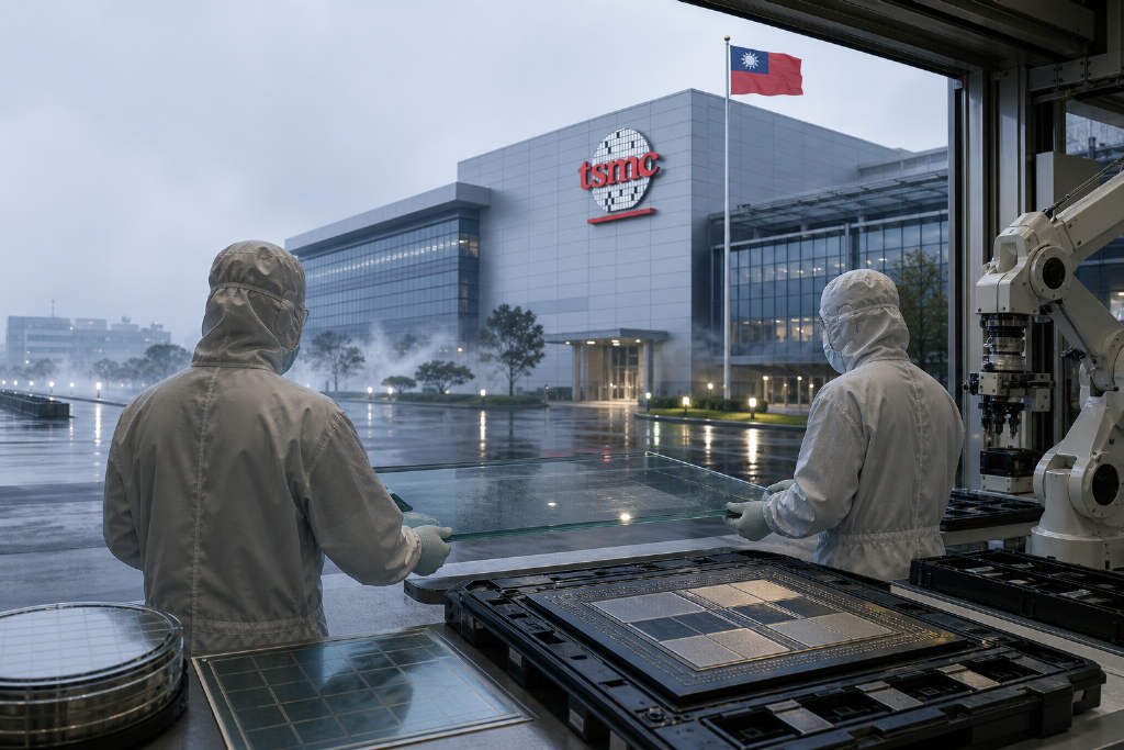
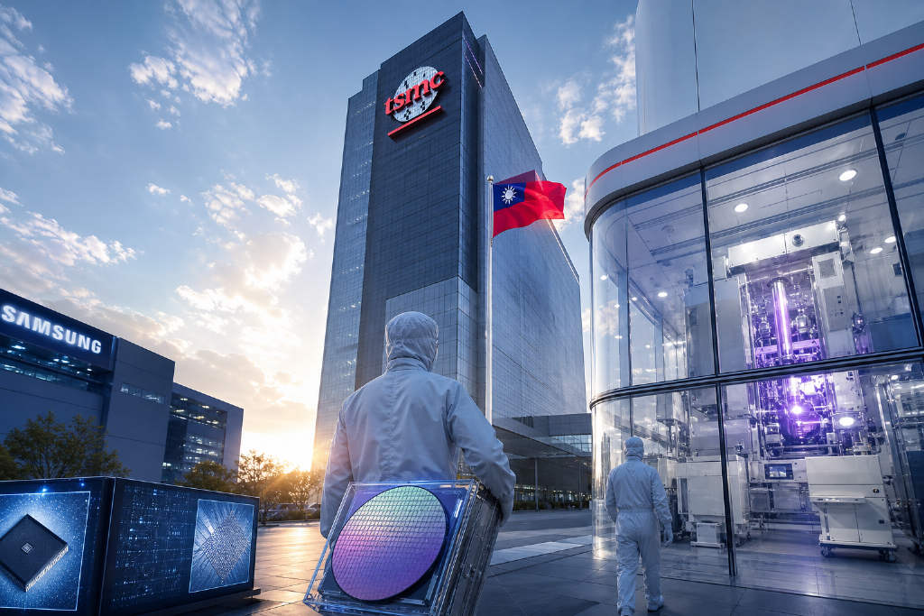
Rising demand for heterogeneous integration in AI chips is pushing package sizes sharply higher, and that has brought glass substrates back into the center of semiconductor discussions. A Statementdog industry report cited by ABMedia says advanced packaging has expanded from "2x reticle" to "4 to 5.5x reticle" in two years, increasing warpage risk and making glass one of the most closely watched material options for next-generation packaging. The report separates two very different uses of glass in packaging: temporary carriers used during manufacturing and removed afterward, and glass substrates or interposers that remain inside the finished product. The second category is drawing most of the market attention. Glass is being considered because it offers adjustable coefficient of thermal expansion, high rigidity, and a very flat surface, traits that can help control warpage and support finer wiring and higher layer counts. At the same time, commercialization still faces major hurdles in TGV reliability, copper adhesion, and inspection methods for transparent material. According to the report, limited commercialization could begin in 2027, possibly in optical communications, while larger-scale production may not arrive until 2028 to 2029. The report says the most important signal for a real volume ramp will be whether Taiwan Semiconductor Manufacturing Co. (TSMC) introduces glass substrates into CoWoS packaging lines, with that window estimated at late 2028 to early 2029.