TSVs

Samsung Elect
2026-09-01 09:22:21

Samsung unveils CUBE 3D memory roadmap with HBM5, zHBM and zNAND-O for AI systems

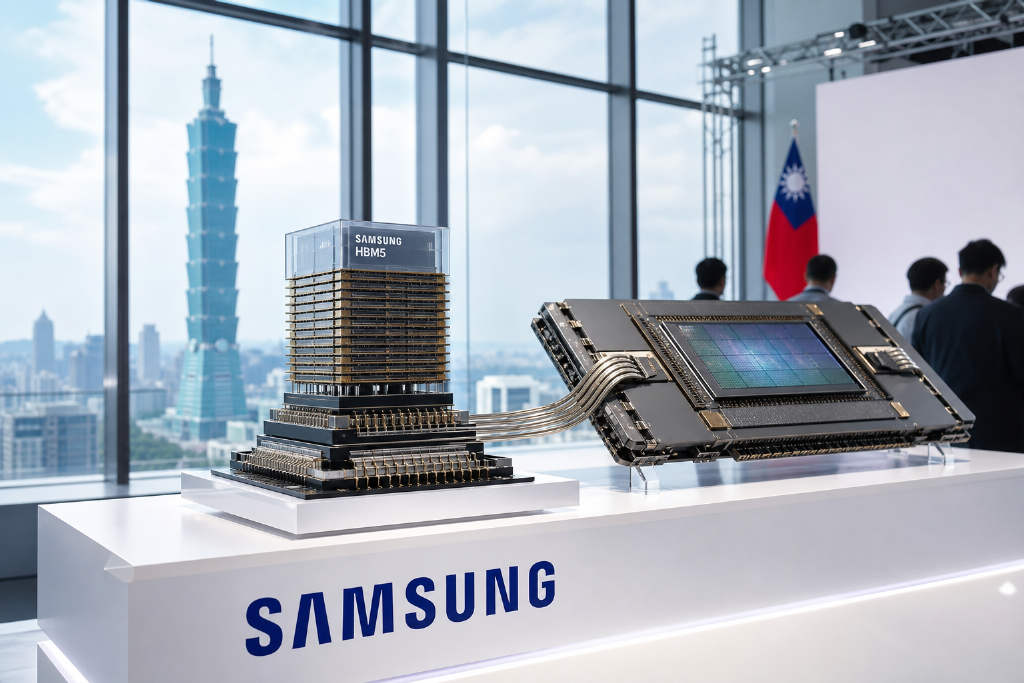
Samsung Electronics used the Memory Executive Summit ahead of SEMICON Taiwan 2026 to lay out a new memory strategy called CUBE, built around a 3D vertical stacking approach. Choi Jang-seok, a vice president in the company’s memory product planning division, said the plan is meant to address rising AI demand for capacity, bandwidth and power efficiency. CUBE stands for Capacity, Utilization, Bandwidth and Efficiency, and Samsung framed it as a way to move past printed circuit board size limits by stacking chips vertically. The company also detailed a three-part roadmap covering HBM5, zHBM and zNAND-O. Samsung said HBM5 is being developed with targets of 2x the performance of HBM4E, a 20% gain in performance per watt and a 20% reduction in thermal resistance. zHBM, first shown last month at FMS 2026 in California, would place HBM directly on top of logic processors such as GPUs or CPUs. Samsung said that design aims for 8x the performance of HBM4E, up to 3x performance per watt and a 75% to 90% drop in thermal resistance. zNAND-O, aimed at large language model storage needs, is designed to stack four or eight layers of V-NAND with TSV and is scheduled to begin sampling in 2028.

1000
Samsung unveils CUBE 3D memory roadmap with HBM5, zHBM and zNAND-O for AI systems
HBF
2026-08-28 01:10:25

Researchers say HBF economics and manufacturing outlook remain unproven

Researchers from P Equity Research and SemiAnalysis, including Nick Doyle, discussed high-bandwidth flash, or HBF, in an X Space, outlining where the technology may fit and where major uncertainties remain. Doyle said it is still too early to judge how much HBF can narrow its cost premium versus high-bandwidth memory, or HBM, because much of the current information comes from vendor claims. He cited Sandisk’s estimate that cost per bit could be about one-eighth that of HBM, while cautioning that structural costs tied to TSVs, stacking, and pSLC mode would not disappear even if yield and testing improve with scale. Endurance remains a central unknown, he said, because higher-than-expected wear would raise overall costs. The discussion also framed HBF as a narrow-use product rather than a replacement for HBM, aimed at AI inference workloads such as low-batch, long-context mixture-of-experts models. Its target bandwidth of about 1.6 TB/s, around HBM3E class, may suit sequential reads for loading model weights and smaller local or private enterprise GPU setups. Thermal reliability and mass production were also flagged as open questions, while NAND shortages are expected to last through 2028.

1000
Researchers say HBF economics and manufacturing outlook remain unproven
SK Hynix
2026-08-24 01:16:47

SK Hynix brings advanced packaging, including Intel EMIB, into next-generation HBM plan

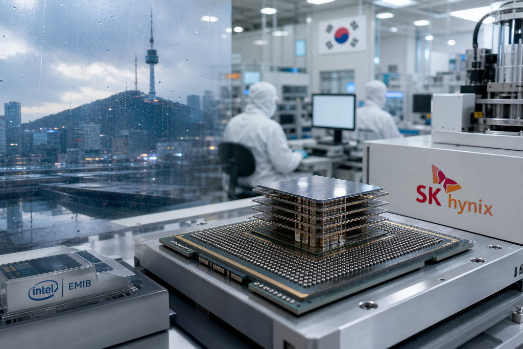
SK Hynix is bringing advanced packaging technologies into its next-generation high-bandwidth memory, or HBM, roadmap, including Intel’s Embedded Multi-die Interconnect Bridge, better known as EMIB. The company also said it ultimately plans to move into the 3D packaging era as it pushes its memory stack design further. At the 2026 Hot Chips conference, Jaesik Lee, vice president of package engineering at SK Hynix, presented a session titled "Advanced Packaging for High-Bandwidth Memory." In that presentation, he detailed how the company intends to use packaging advances to speed up its HBM product roadmap. SK Hynix is currently exploring methods such as hybrid bonding to break past the 16-layer stacking limit. Looking ahead, the company also plans to address power consumption challenges by increasing the number of through-silicon vias, improving IO speed for logic process integration, and optimizing the power delivery network, or PDN. As of publication, SK Hynix shares in South Korea were up 1.71%.

2180
SK Hynix brings advanced packaging, including Intel EMIB, into next-generation HBM plan
Intel
2026-08-04 08:15:44

Intel’s EMIB-T nears 90% yield with packaging costs about half of TSMC CoWoS

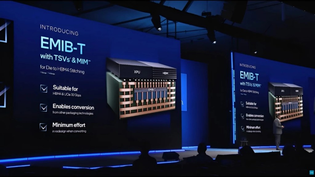
Intel’s EMIB-T advanced packaging technology is moving closer to commercialization, with industry sources cited by ABMedia saying packaging yield is approaching 90% and total packaging quotes are roughly 40% to 50% below Taiwan Semiconductor Manufacturing Co.’s CoWoS offering. The design replaces the large silicon interposer used in CoWoS with an embedded silicon bridge inside an organic substrate, and the EMIB-T version adds through-silicon vias, or TSVs, to route power and high-speed signals vertically for 3D stacking. The report said packaging-side maturity is already high, while substrate production remains the main obstacle. Substrate yield is still around 50%, making it the key technical bottleneck before volume production. EMIB-T is expected to enter formal mass production in 2027, with ASIC makers and developers of CPU-based AI chips seen as the main target customers because of the lower cost profile. ABMedia also said Intel is pushing ahead with its Ohio wafer fab project, a more than 1,000-acre manufacturing site tied to the company’s Angstrom-generation 18A and 14A nodes. Wccftech said Intel has begun paying overtime bonuses to on-site workers as it works toward large-scale 14A production in 2031.

2500
Intel’s EMIB-T nears 90% yield with packaging costs about half of TSMC CoWoS
SK hynix
2026-07-24 08:44:16

SK hynix pushes 3D stacked DRAM for on-device AI, with Apple named as a likely partner

SK hynix has begun laying the groundwork to commercialize 3D stacked DRAM-on-Logic technology for next-generation on-device AI memory, according to the source article. The company is recruiting design engineers through its U.S. subsidiary in California, and a job description cited by Korean media says the work involves close collaboration with a U.S. customer on co-designing 3D stacked DRAM logic chips. Citrini analyst Jukan identified Apple as the most likely partner, arguing that Apple’s long-running in-house A-series and M-series chip development, its focus on package-level integration, and its existing memory ties with SK hynix make it a plausible fit. The report frames 3D stacked DRAM as a potential answer to the limits of current PoP smartphone packaging, which struggles to deliver the bandwidth, power efficiency, and space utilization needed for on-device AI inference. At the same time, the article stresses that broad commercialization remains distant, with technical maturity, production readiness, and supply-chain alignment still ahead.

180
SK hynix pushes 3D stacked DRAM for on-device AI, with Apple named as a likely partner