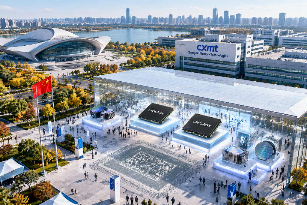
CXMT says G5 DRAM platform has entered mass production, with economics still under scrutiny
Changxin Memory Technologies, or CXMT, said at the 2026 World Manufacturing Convention on Sept. 20 that its fifth-generation DRAM technology platform, G5, has entered mass production, alongside two 24Gb LPDDR5X products built on the node. The company highlighted four figures: an 11.95 nm active-area half-pitch, a capacitor aspect ratio of 45:1, a 6,762 nm core functional area height, and at least a 50% increase in dies per wafer versus the prior generation. The announcement matters less because of the “fifth-generation” label than because of how CXMT got there. The article argues that, without access to EUV lithography tools in mainland China, the company has pushed its process to roughly the industry’s 1c-class range using DUV multi-patterning and a broader stack of process modules, including HKMG and other structural changes. That said, node alignment does not mean cost alignment. The reported 50% gain refers to dies per wafer on an 8Gb-equivalent basis before yield screening, not to sellable output. CXMT did not disclose G5 yield or monthly production. The piece says the real questions now are how quickly yield improves, how fast cost per bit converges with the three global leaders, and whether HBM can move from reported trial production to an officially confirmed product line.