TSV

Policy and Re
2026-09-18 02:05:26

SEC unveils tokenized stock exemption as Atkins pushes longer U.S. stock trading hours

The U.S. Securities and Exchange Commission rolled out a temporary, conditional "Innovation Exemption" that allows limited on-chain trading of certain tokenized stocks through qualified tokenized securities venues, while setting guardrails that ban synthetic tokenized equities. SEC Chair Paul S. Atkins said the agency is also preparing for longer U.S. equity trading hours, arguing that tokenization could support real-time inventory management, improve efficiency, cut settlement failures, and reduce naked short-selling risk. The day’s broader crypto and market roundup also included Grayscale’s view that the latest Federal Reserve rate hike looks more like a mid-cycle adjustment than a major policy turn, new volume data from Hyperliquid’s HIP-3 markets, Ethereum’s Glamsterdam Devnet-11 rehearsal, an oracle attack on Nostra, MoonPay’s plan to use the $1.2 billion WTGXX tokenized money market fund in stablecoin reserve management, Robinhood Chain crossing 750 million transactions, and Tenka’s $2 million Pre-Seed financing led by Maven 11. Market data showed ZEC briefly topped $1,500 and set another all-time high, while major centralized exchange gainers included NEAR, ARB, UNI, and ZEC.


450
SEC unveils tokenized stock exemption as Atkins pushes longer U.S. stock trading hours
SEC
2026-09-18 05:00:35

SEC opens limited trading path for tokenized stocks through TSV exemption

The U.S. Securities and Exchange Commission has created a limited route for tokenized stock trading by granting a temporary, conditional “Innovation Exemption” for Tokenized Securities Venues, or TSVs. Under the framework, tokenized National Market System stocks may trade on approved on-chain venues, but only under strict conditions. TSVs must be U.S. entities, comply with Office of Foreign Assets Control sanctions rules, restrict access to eligible participants, and bar synthetic tokenized equities. Token holders must receive the same rights as traditional shareholders, including dividends and voting rights, while issuers retain the right to object and block trading of their securities on a TSV. The exemption takes effect immediately and runs for five years, to around September 2031, while the SEC seeks public comment on possible rule changes. The agency also set detailed limits on product design, trading halts, smart contract disclosure, and volume caps for Tier1 and Tier2 stocks. SEC Commissioner Hester M. Peirce separately outlined six open questions tied to overnight trading, disclosure timing, broker obligations, and investor protection. After the announcement, Robinhood CEO Vlad Tenev and AMC CEO Adam Aron both welcomed the framework, and several crypto assets tied to tokenization and DeFi posted gains.

350
SEC opens limited trading path for tokenized stocks through TSV exemption
YMTC
2026-09-16 01:05:14

Korean industry assessment says China’s memory chip gap has narrowed to about 1 year in NAND and 2 years in DRAM

A new assessment from the Korea Semiconductor Industry Association says the technology gap between Chinese memory makers and leading global suppliers has narrowed much faster than previously believed. According to the evaluation, Yangtze Memory Technologies Co. (YMTC) trails top players by about one year in NAND flash, while ChangXin Memory Technologies (CXMT) is roughly two years behind in DRAM and about three years behind in high-bandwidth memory, or HBM. The report says the gap had widely been viewed as around five years not long ago. The article, citing JoongAng Ilbo and the Korean industry group, also lays out a series of product and capacity milestones. It says Samsung Electronics and SK hynix began producing 300-layer NAND in 2025 while YMTC was at 270 layers, and that YMTC is expected to move to 400-layer NAND by 2027. In DRAM, Samsung and SK hynix started DDR5 production in 2023, while CXMT began DDR5 memory module production in 2025. The report adds that CXMT has already started mass production of LPDDR5X and has just begun producing LPDDR6. On HBM, the piece says CXMT has started trial production of HBM3E modules with yields of about 25%, while continuing to work through TSV-related manufacturing challenges. It also says both CXMT and YMTC may be pursuing competitive architectures without relying on EUV lithography, even as domestic DUV tool makers still face bottlenecks in projection lenses and light sources.

660
Korean industry assessment says China’s memory chip gap has narrowed to about 1 year in NAND and 2 years in DRAM
3D DRAM
2026-09-14 11:09:11

3D DRAM race heats up as AMD, NAURA and memory giants push new architectures and process tools

Two developments in the first week of September 2026 put 3D DRAM back at the center of the memory industry. AMD disclosed internal test results for a Hybrid Bonding-based 3D DRAM architecture, saying energy efficiency could improve by as much as 17x versus conventional HBM stacks. Around the same time, Chinese semiconductor equipment maker NAURA published an IEEE paper describing a manufacturing advance for next-generation 3D DRAM, including a two-step cyclic etch process for 64-layer alternating silicon and silicon-germanium structures, structural uniformity above 95%, an etch selectivity above 500:1, and silicon loss below 10 angstroms in a 200 nm interlayer structure. The report argues that these announcements matter because conventional DRAM scaling is nearing physical and economic limits. It also reviews the two main technical paths now being pursued, 4F2 VCT and VS-CAT, and outlines how Samsung Electronics, SK hynix, and Micron are positioning themselves. Beyond chipmakers, the shift is also reshaping the equipment chain, from high-aspect-ratio etch to atomic layer deposition, wafer bonding, CMP, cleaning, inspection, coating and developing, testing, and high-purity process systems.

1090
3D DRAM race heats up as AMD, NAURA and memory giants push new architectures and process tools
CXMT
2026-09-09 12:35:00

Report says CXMT HBM3 yield is 25%, with nearly 80 out of 100 units failing final testing

Chinese memory maker ChangXin Memory Technologies, or CXMT, is reported to be seeing a 25% yield rate on HBM3, according to a Sept. 9 report by The Chosun Daily cited by Chip Briefing. Using an eight-layer HBM3 stack as the basis, the report said nearly 80 out of every 100 chips fail to clear final testing. The report broke the figure into two stages. Front-end process yield was said to be around 30%, and only about 70% of the units that advanced to back-end packaging and testing passed final inspection. Multiplying those two stages results in an overall yield of roughly 25%. Industry sources in the report described 80% as the usual threshold for mass production, putting CXMT’s reported level at about one-third of that benchmark. As a comparison, the report said SK hynix has maintained HBM3 yields above 90% since entering mass production in 2022. The figures were not disclosed by CXMT itself. The Chosun Daily attributed them to an unnamed senior executive in the semiconductor equipment industry who was said to be familiar with the company’s situation.

950
Report says CXMT HBM3 yield is 25%, with nearly 80 out of 100 units failing final testing
CXMT
2026-09-09 00:23:43

CXMT starts HBM3 pilot production with initial yields at about 25%, report says

Chinese DRAM maker ChangXin Memory Technologies, or CXMT, has started pilot production of fourth-generation high-bandwidth memory HBM3, with initial yields stalled at 25%, according to a report by The Chosun Daily cited by ChainCatcher. The report said that level is roughly one-third of the 80% yield often seen as a target for mass production. SK Hynix has been mass-producing similar products since 2022, with yields above 90%. For CXMT’s 8-layer HBM3 stack, front-end process yields were reported at about 30%, while roughly 70% made it through the back-end process as final good units. The company has supplied a small number of samples to Chinese firms including Alibaba’s T-Head and Cambricon, and is continuing to improve yields. The report added that CXMT’s G4, a 17nm-class process, does not face major issues in conventional DRAM production, but HBM requires larger DRAM die and tighter electrical specifications. Industry sources in the report pointed to limited maturity in through-silicon via, or TSV, technology. Analysis from Nomad Semi said Samsung’s HBM2 has more than 5,000 TSVs per chip, SK Hynix’s HBM3 has more than 8,000, and CXMT has about 3,000, leaving the company 4 to 5 years behind Samsung and SK Hynix.

820
CXMT starts HBM3 pilot production with initial yields at about 25%, report says
ChainCatcher
2026-09-07 02:27:19

Research note says China’s memory push is now split across CXMT, YMTC and XMC

A research note from Schulz_Research said China’s memory buildout is no longer centered on a single company, but on a three-part structure led by CXMT, YMTC and XMC. In the note, CXMT is described as handling DRAM wafers, while YMTC focuses on NAND and is adding DRAM at its newest plant. XMC, a foundry controlled by YMTC, is tasked with stacking products from both lines. The post linked that structure to rules Beijing has applied since late December last year. Under those rules, newly approved factories must show in procurement tenders that at least half of their equipment is sourced domestically, with exemptions granted only when no domestic option is available. Schulz_Research said YMTC’s Wuhan Phase 3 is the first advanced memory project cleared under that framework and is set to begin production later this year. The note also outlined capacity figures for CXMT, YMTC and XMC, alongside market-share estimates and product updates including DDR5, LPDDR5 and planned HBM3 production.

930
Research note says China’s memory push is now split across CXMT, YMTC and XMC
Samsung Elect
2026-09-01 09:22:21

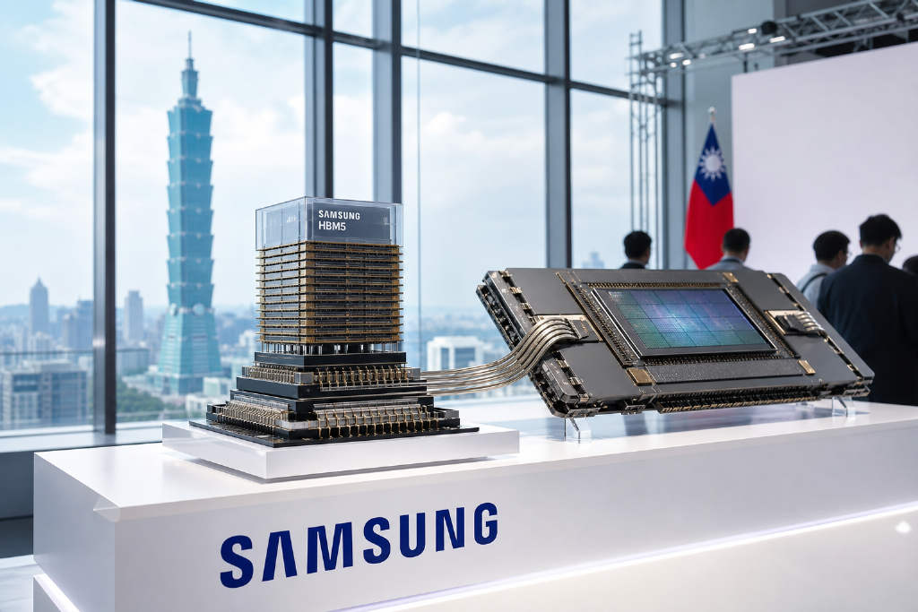
Samsung unveils CUBE 3D memory roadmap with HBM5, zHBM and zNAND-O for AI systems

Samsung Electronics used the Memory Executive Summit ahead of SEMICON Taiwan 2026 to lay out a new memory strategy called CUBE, built around a 3D vertical stacking approach. Choi Jang-seok, a vice president in the company’s memory product planning division, said the plan is meant to address rising AI demand for capacity, bandwidth and power efficiency. CUBE stands for Capacity, Utilization, Bandwidth and Efficiency, and Samsung framed it as a way to move past printed circuit board size limits by stacking chips vertically. The company also detailed a three-part roadmap covering HBM5, zHBM and zNAND-O. Samsung said HBM5 is being developed with targets of 2x the performance of HBM4E, a 20% gain in performance per watt and a 20% reduction in thermal resistance. zHBM, first shown last month at FMS 2026 in California, would place HBM directly on top of logic processors such as GPUs or CPUs. Samsung said that design aims for 8x the performance of HBM4E, up to 3x performance per watt and a 75% to 90% drop in thermal resistance. zNAND-O, aimed at large language model storage needs, is designed to stack four or eight layers of V-NAND with TSV and is scheduled to begin sampling in 2028.

1000
Samsung unveils CUBE 3D memory roadmap with HBM5, zHBM and zNAND-O for AI systems